
Page 33 - Microsensors, MEMS and Smart Devices - Gardner Varadhan and Awadelkarim
P. 33
PATTERN TRANSFER 15
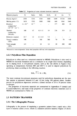
Table 2.2 Properties of some selected electronic materials
Material property Si GaAs SiO 2 Si 3N 4 Al Au Ti
3
Density (kg/m ) 2330 5316 1544 3440 2699 19320 4508
Melting point (°C) 1410 1510 1880 1900 660 1064 1660
Electrical 4 x 10 -5 10 -11 - - 377 488 26
conductivity"
-1
-1
(10 3 W cm )
Thermal 168 47 6.5-11 19 236 319 22
conductivity
(W/m/K)
Dielectric constant 11.7 12 4.3-4.5 7.5 - - -
Young's modulus 190 - 380 380 70 78 -40
(GPa)
Yield strength 6.9 — 14 14 50 200 480
(GPa)
"Measured at room temperature. Some other properties will vary with temperature
2.2.3 Polysilicon Film Deposition
Polysilicon is often used as a structural material in MEMS. Polysilicon is also used in
MEMS for electrode formation and as a conductor or as a high-value resistor, depending
on its doping level. A low-pressure reactor, such as the one shown in Figure 2.3(a),
operating at temperatures between 600 and 650 °C is used to deposit poly silicon by
pyrolysing silane according to the following reaction:
600°C
(2.6)
SiH 4 Si + 2H 2
The most common low-pressure processes used for polysilicon deposition are the ones
that operate at pressures between 0.2 and 1.0 torr using 100 percent silane. Another
process for polysilicon deposition involves a diluted mixture of 20 to 30 percent silane
in nitrogen.
The properties of electronic materials are summarised in Appendices F (metals) and
G (semiconductors), and some of the properties of common electronic materials used in
MEMS are summarised in Table 2.2.
2.3 PATTERN TRANSFER
2.3.1 The Lithographic Process
Lithography is the process of imprinting a geometric pattern from a mask onto a thin
layer of material called a resist, which is a radiation-sensitive material. Figure 2.5 shows