
Page 29 - Microsensors, MEMS and Smart Devices - Gardner Varadhan and Awadelkarim
P. 29
ELECTRONIC MATERIALS AND THEIR DEPOSITION 11
Thermal oxidation of silicon in oxygen or water vapour can be described by the
following two chemical reactions:
900- 1200°C
Si (solid) + O 2 (gas) > SiO 2 (solid) (2.1)
and
900- 1200 °C
Si (solid) + 2H 2O (gas) SiO 2 (solid) + 2H 2 (gas) (2.2)
The silicon-silicon dioxide interface transverses the silicon during the oxidation process.
Using the densities and molecular weights of silicon and SiO 2, it can be shown that
growing an oxide of thickness x consumes a layer of silicon that is 0.44x thick.
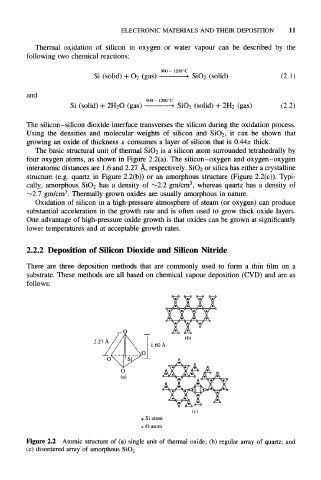
The basic structural unit of thermal SiO 2 is a silicon atom surrounded tetrahedrally by
four oxygen atoms, as shown in Figure 2.2(a). The silicon-oxygen and oxygen-oxygen
interatomic distances are 1.6 and 2.27 A, respectively. SiO 2 or silica has either a crystalline
structure (e.g. quartz in Figure 2.2(b)) or an amorphous structure (Figure 2.2(c)). Typi-
3
cally, amorphous SiO 2 has a density of ~2.2 gm/cm , whereas quartz has a density of
3
~2.7 gm/cm . Thermally grown oxides are usually amorphous in nature.
Oxidation of silicon in a high-pressure atmosphere of steam (or oxygen) can produce
substantial acceleration in the growth rate and is often used to grow thick oxide layers.
One advantage of high-pressure oxide growth is that oxides can be grown at significantly
lower temperatures and at acceptable growth rates.
2.2.2 Deposition of Silicon Dioxide and Silicon Nitride
There are three deposition methods that are commonly used to form a thin film on a
substrate. These methods are all based on chemical vapour deposition (CVD) and are as
follows:
Figure 2.2 Atomic structure of (a) single unit of thermal oxide; (b) regular array of quartz; and
(c) disordered array of amorphous SiO2