
Page 28 - Microsensors, MEMS and Smart Devices - Gardner Varadhan and Awadelkarim
P. 28
10 ELECTRONIC MATERIALS AND PROCESSING
1. Thermal silicon oxide
2. Dielectric layers
3. Poly crystalline silicon (poly-Si)
4. Metal films (predominantly aluminum)
The dielectric layers include deposited silicon dioxide (SiO 2) (sometimes referred to
as oxide) and silicon nitride (Si 3N 4). These dielectrics are used for insulation between
conducting layers, for diffusion and ion-implantation masks, and for passivation to protect
devices from impurities, moisture, and scratches. Poly-Si is used as a gate electrode in
metal oxide semiconductor (MOS) devices, as a conductive material for multilevel metalli-
sation, and as a contact material for devices with shallow junctions. Metal films are used
+
to form low-resistance ohmic connections, both to heavily doped n /p + regions and to
poly-Si layers, and rectifying (nonohmic) contacts in metal semiconductor barriers.
The thermal oxide is usually a better-quality oxide (compared with deposited oxide) and
is used for the gate oxide layers in field-effect transistors (FETs). A detailed description
of FET devices and their electrical characteristics is given in Chapter 4.
As shall become apparent in the following chapters, electronic materials are of major
importance in MEMS devices. Therefore, the methods used for growing thermal SiOa and
for depositing dielectric poly-Si and metallic layers are reviewed in the following sections.
2.2.1 Oxide Film Formation by Thermal Oxidation
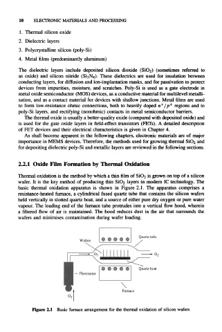
Thermal oxidation is the method by which a thin film of SiO 2 is grown on top of a silicon
wafer. It is the key method of producing thin SiO 2 layers in modern IC technology. The
basic thermal oxidation apparatus is shown in Figure 2.1. The apparatus comprises a
resistance-heated furnace, a cylindrical fused quartz tube that contains the silicon wafers
held vertically in slotted quartz boat, and a source of either pure dry oxygen or pure water
vapour. The loading end of the furnace tube protrudes into a vertical flow hood, wherein
a filtered flow of air is maintained. The hood reduces dust in the air that surrounds the
wafers and minimises contamination during wafer loading.
Figure 2.1 Basic furnace arrangement for the thermal oxidation of silicon wafers