
Page 35 - Microsensors, MEMS and Smart Devices - Gardner Varadhan and Awadelkarim
P. 35
17
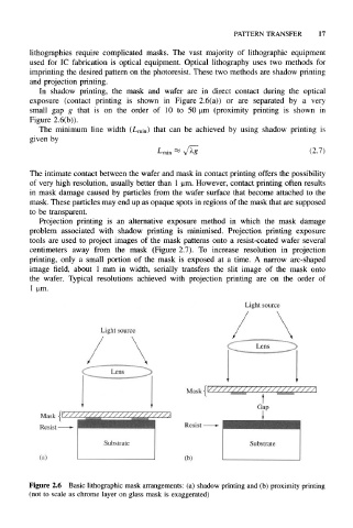
lithographies require complicated masks. The vast majority of lithographic equipment
used for IC fabrication is optical equipment. Optical lithography uses two methods for
imprinting the desired pattern on the photoresist. These two methods are shadow printing
and projection printing.
In shadow printing, the mask and wafer are in direct contact during the optical
exposure (contact printing is shown in Figure 2.6(a)) or are separated by a very
small gap g that is on the order of 10 to 50 urn (proximity printing is shown in
Figure 2.6(b)).
The minimum line width (L min) that can be achieved by using shadow printing is
given by
(2.7)
The intimate contact between the wafer and mask in contact printing offers the possibility
of very high resolution, usually better than 1 jam. However, contact printing often results
in mask damage caused by particles from the wafer surface that become attached to the
mask. These particles may end up as opaque spots in regions of the mask that are supposed
to be transparent.
Projection printing is an alternative exposure method in which the mask damage
problem associated with shadow printing is minimised. Projection printing exposure
tools are used to project images of the mask patterns onto a resist-coated wafer several
centimeters away from the mask (Figure 2.7). To increase resolution in projection
printing, only a small portion of the mask is exposed at a time. A narrow arc-shaped
image field, about 1 mm in width, serially transfers the slit image of the mask onto
the wafer. Typical resolutions achieved with projection printing are on the order of
1 urn.
Figure 2.6 Basic lithographic mask arrangements: (a) shadow printing and (b) proximity printing
(not to scale as chrome layer on glass mask is exaggerated)