
Page 38 - Microsensors, MEMS and Smart Devices - Gardner Varadhan and Awadelkarim
P. 38
20 ELECTRONIC MATERIALS AND PROCESSING
the surface of a wafer, which is pressure-attached to a wafer holder through holes in the
holder that are connected to a vacuum line, and continuously pumped during the process.
The wafer holder itself is attached to and spun by a motor. The thickness jc of the spin-on
material is related to the viscosity n of the liquid and the solid content / in the solution
as well as the spin speed w:
nf
(2.8)
Typical spin speeds are in the range 1000–10000 rpm to give material thickness in the
range of 0.5 to 1 um. After the wafer is spin-coated with the resist solution, it is dried
and baked at temperatures in the range of 90 to 450 °C, depending on the type of the
resist. Baking is necessary for further drying of the resist and for strengthening the resist
adhesion to the wafer (Table 2.3).
A resist is a radiation-sensitive material that can be classified as positive or negative,
depending on how it responds to radiation. The positive resist is rendered soluble in a
developer when it is exposed to radiation. Therefore, after exposure to radiation, a positive
resist can be easily removed in the development process (dissolution of the resist in an
appropriate solvent, which is sometimes called the developer). The net effect is that the
patterns formed (also called images) in the positive resist are the same as those formed
on the mask (Figure 2.10). A negative resist, on the other hand, is rendered less soluble
in a developer when it is exposed to radiation. The patterns formed in a negative resist
are thus the reverse of those formed on the mask patterns (Figure 2.10). Table 2.4 lists a
few of the commercially available resists, the lithographic process, and their polarity (see
Table 4.3).
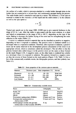
Table 23 Some properties of the common spin-on materials
Material Thickness (um) Bake temperature (°C) Solvent
Photoresist 0.1-10 90-150 Weak base
Polyimide 0.3-100 350-450 Weak base
Silicon dioxide 0.1-0.5 500-900 HF
Lead titanate 0.1-0.3 650 HNO 3
Table 2.4 Commercially available resists
Resist Lithography Type
Kodak 747 Optical Negative
AZ-1350J Optical Positive
PR 102 Optical Positive
Poly(methyl methacrylate) (PMMA) E-beam and X ray Positive
Poly[(glycidyl methacrylate)-co- E-beam and X ray Negative
ethylacrylate] (COP)
Dichloropropyl acrylate and glycidyl Xray Negative
methacrylate-co-ethyl acrylate (DCOPA)