
Page 177 - Multifunctional Photocatalytic Materials for Energy
P. 177
Metal-based semiconductor nanomaterials for thin-film solar cells 163
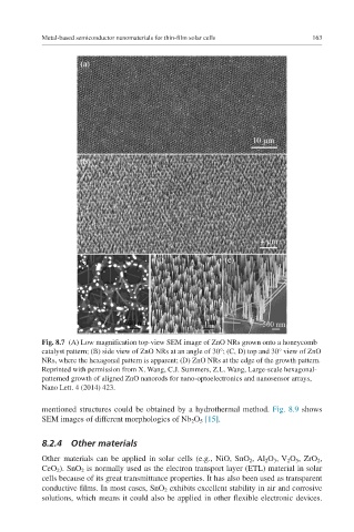
Fig. 8.7 (A) Low magnification top-view SEM image of ZnO NRs grown onto a honeycomb
catalyst pattern; (B) side view of ZnO NRs at an angle of 30°; (C, D) top and 30° view of ZnO
NRs, where the hexagonal pattern is apparent; (D) ZnO NRs at the edge of the growth pattern.
Reprinted with permission from X. Wang, C.J. Summers, Z.L. Wang, Large-scale hexagonal-
patterned growth of aligned ZnO nanorods for nano-optoelectronics and nanosensor arrays,
Nano Lett. 4 (2014) 423.
mentioned structures could be obtained by a hydrothermal method. Fig. 8.9 shows
SEM images of different morphologies of Nb 2 O 5 [15].
8.2.4 Other materials
Other materials can be applied in solar cells (e.g., NiO, SnO 2 , Al 2 O 3 , V 2 O 5 , ZrO 2 ,
CeO 2 ). SnO 2 is normally used as the electron transport layer (ETL) material in solar
cells because of its great transmittance properties. It has also been used as transparent
conductive films. In most cases, SnO 2 exhibits excellent stability in air and corrosive
solutions, which means it could also be applied in other flexible electronic devices.