
Page 180 - Multifunctional Photocatalytic Materials for Energy
P. 180
166 Multifunctional Photocatalytic Materials for Energy
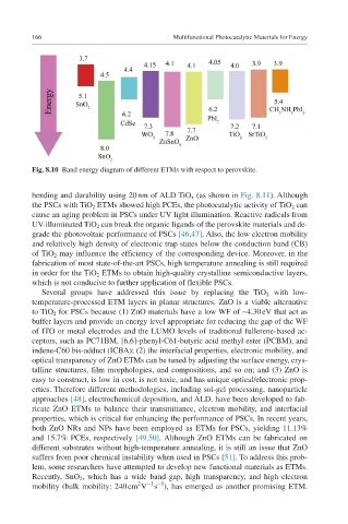
Fig. 8.10 Band energy diagram of different ETMs with respect to perovskite.
bending and durability using 20 nm of ALD TiO x (as shown in Fig. 8.11). Although
the PSCs with TiO 2 ETMs showed high PCEs, the photocatalytic activity of TiO 2 can
cause an aging problem in PSCs under UV light illumination. Reactive radicals from
UV-illuminated TiO 2 can break the organic ligands of the perovskite materials and de-
grade the photovoltaic performance of PSCs [46,47]. Also, the low electron mobility
and relatively high density of electronic trap states below the conduction band (CB)
of TiO 2 may influence the efficiency of the corresponding device. Moreover, in the
fabrication of most state-of-the-art PSCs, high temperature annealing is still required
in order for the TiO 2 ETMs to obtain high-quality crystalline semiconductive layers,
which is not conducive to further application of flexible PSCs.
Several groups have addressed this issue by replacing the TiO 2 with low-
temperature- processed ETM layers in planar structures. ZnO is a viable alternative
to TiO 2 for PSCs because (1) ZnO materials have a low WF of ~4.30 eV that act as
buffer layers and provide an energy level appropriate for reducing the gap of the WF
of ITO or metal electrodes and the LUMO levels of traditional fullerene-based ac-
ceptors, such as PC71BM, [6,6]-phenyl-C61-butyric acid methyl ester (PCBM), and
indene-C60 bis-adduct (ICBA); (2) the interfacial properties, electronic mobility, and
optical transparency of ZnO ETMs can be tuned by adjusting the surface energy, crys-
talline structures, film morphologies, and compositions, and so on; and (3) ZnO is
easy to construct, is low in cost, is not toxic, and has unique optical/electronic prop-
erties. Therefore different methodologies, including sol-gel processing, nanoparticle
approaches [48], electrochemical deposition, and ALD, have been developed to fab-
ricate ZnO ETMs to balance their transmittance, electron mobility, and interfacial
properties, which is critical for enhancing the performance of PSCs. In recent years,
both ZnO NRs and NPs have been employed as ETMs for PSCs, yielding 11.13%
and 15.7% PCEs, respectively [49,50]. Although ZnO ETMs can be fabricated on
different substrates without high-temperature annealing, it is still an issue that ZnO
suffers from poor chemical instability when used in PSCs [51]. To address this prob-
lem, some researchers have attempted to develop new functional materials as ETMs.
Recently, SnO 2 , which has a wide band gap, high transparency, and high electron
−1 −1
2
mobility (bulk mobility: 240 cm V s ), has emerged as another promising ETM.