
Page 210 - Multifunctional Photocatalytic Materials for Energy
P. 210
Metal-based semiconductor nanomaterials for photocatalysis 195
Oscillating electron cloud
Electric field
e − e − e − −
e − e
+ ++ + Metal
nanoparticle
Metal
nanoparticle
Magnetic ++ ++
field e − e −
− − −
e e e
e − e −
E cb
E vb
Semiconductor
particle
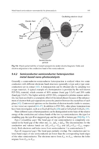
Fig. 9.6 Dipole polarizability of metal nanoparticles under electric/magnetic fields and
electron migration to the conduction band of the semiconductor.
9.4.2 Semiconductor-semiconductor heterojunction
metal-based nano-photocatalysts
Generally a semiconductor-semiconductor heterojunction is realized when two semi-
conductors with different electronic band structures (generally n-type and p-type semi-
conductors) are in contact [42]. A homojunction can be obtained also by adopting two
n-type materials. A typical example of a homojunction is provided by the well-known
P25-TiO 2 material, which consists of 80% anatase (band gap 3.2 eV) and 20% rutile
(band gap 3.0 eV). The higher activity of P25-TiO 2 , compared to pristine anatase and ru-
tile, has been ascribed to a synergistic effect of the mixed phases because of the enhance-
ment of electron-hole pair separations across the junction between the crystallites of each
phase [43]. Controversial opinions on the direction of electron transfer (rutile-to-anatase,
or vice versa) are reported [44–47]. In addition to P25-TiO 2 , other phase homojunctions
have been investigated, such as α-Ga 2 O 3 /β-Ga 2 O 3 [48] and α-CaTa 2 O 6 /β-CaTa 2 O 6 [49].
Three different types of heterojunctions can be distinguished on the basis of the relative
energy of the conduction and valence bands of the two n-p semiconductors: the type-I or
straddling gap, the type-II or staggered gap, and the type-III or broken gap [50] (Fig. 9.7).
Type-I (straddling gap): The band gap of one semiconductor is completely con-
tained in the band gap of the other one, i.e., ΔE g1 > ΔE g2 . The discontinuities for the
conduction and valence bands are ΔE cb = E cb1 − E cb2 and ΔE vb = E vb1 − E vb2 , respec-
tively. Both electrons and holes move from semiconductor 1 to semiconductor 2.
Type-II (staggered gap): The band gaps partially overlap. The conduction and va-
lence band-edges of one semiconductor are lower than the corresponding band-edges
of the other semiconductor. The electrons move from E cb1 to E cb2 , whereas the holes
migrate from E vb2 to E vb1 .