
Page 235 - Multifunctional Photocatalytic Materials for Energy
P. 235
218 Multifunctional Photocatalytic Materials for Energy
+
–
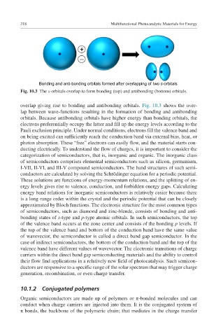
Bonding and anti-bonding orbitals formed after overlapping of two s-orbitals
Fig. 10.3 The s-orbitals overlap to form bonding (top) and antibonding (bottom) orbitals.
overlap giving rise to bonding and antibonding orbitals. Fig. 10.3 shows the over-
lap between wave-functions resulting in the formation of bonding and antibonding
orbitals. Because antibonding orbitals have higher energy than bonding orbitals, the
electrons preferentially occupy the latter and fill up the energy levels according to the
Pauli exclusion principle. Under normal conditions, electrons fill the valence band and
on being excited can sufficiently reach the conduction band via external bias, heat, or
photon absorption. These “free” electrons can easily flow, and the material starts con-
ducting electrically. To understand the flow of charges, it is important to consider the
categorization of semiconductors, that is, inorganic and organic. The inorganic class
of semiconductors comprises elemental semiconductors such as silicon, germanium,
I-VII, II-VI, and III-V compound semiconductors. The band structures of such semi-
conductors are calculated by solving the Schrödinger equation for a periodic potential.
These solutions are functions of energy-momentum relations, and the splitting of en-
ergy levels gives rise to valence, conduction, and forbidden energy gaps. Calculating
energy band relations for inorganic semiconductors is relatively easier because there
is a long-range order within the crystal and the periodic potential that can be closely
approximated by Bloch functions. The electronic structure for the most common types
of semiconductors, such as diamond and zinc-blende, consists of bonding and anti-
bonding states of s-type and p-type atomic orbitals. In such semiconductors, the top
of the valence band occurs at the zone center and consists of the bonding p levels. If
the top of the valence band and bottom of the conduction band have the same value
of wavevector, the semiconductor is called a direct band gap semiconductor. In the
case of indirect semiconductors, the bottom of the conduction band and the top of the
valence band have different values of wavevector. The electronic transitions of charge
carriers within the direct band gap semiconducting materials and the ability to control
their flow find applications in a relatively new field of photocatalysis. Such semicon-
ductors are responsive to a specific range of the solar spectrum that may trigger charge
generation, recombination, or even charge transfer.
10.1.2 Conjugated polymers
Organic semiconductors are made up of polymers or π-bonded molecules and can
conduct when charge carriers are injected into them. It is the conjugated system of
π bonds, the backbone of the polymeric chain; that mediates in the charge transfer