
Page 92 - Multifunctional Photocatalytic Materials for Energy
P. 92
Graphene photocatalysts 81
route toward the large-scale production of graphene for different applications [22]
(Fig. 5.1C). Furthermore, rGO offers an important advantage, namely the possibility
to obtain a tailored hydrophilic surface of graphene decorated with oxygenated func-
tionalities, which results in low production costs [19,20]. These surface groups can be
used to facilitate the anchoring of semiconductors and metal nanoparticles and even
for the assembly of macroscopic structures, which are relevant to developing highly
efficient photocatalysts [23,24].
Heteroatom doping of graphene is a rising research approach toward enhancing
the performance of graphene-based materials for a wide range of applications [25],
which presents an opportunity to further extend the role of graphene in photocatalysis
[26]. In heteroatom-doped graphene materials, a certain percentage of carbon atoms
(typically below 10 wt.%) is replaced by other elements, such as nitrogen (N) [27–29],
boron (B) [30], phosphorus (P) [31], and sulfur (S) [32,33] (Fig. 5.1D). Several pos-
sibilities exist for preparing doped-graphene materials, such as CVD; arc-discharge
between two graphite electrodes in the presence of a suitable reagent containing the
dopant element, for example, NH 3 and H 2 S; ball-milling; and pyrolysis under inert at-
mosphere of a natural biopolymer [34]. It is worth noting that the presence of external
atoms and defects in graphene is a critical point in catalysis applications. Indeed, the
main graphene materials that have been applied in photocatalysis are GO, rGO, and
doped-graphene derivatives [25,26].
5.2.1 General properties of graphene-based materials
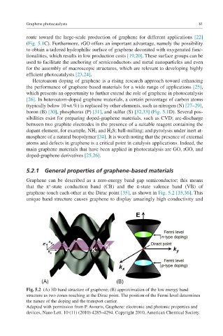
Graphene can be described as a zero-energy band gap semiconductor; this means
⁎
that the π -state conduction band (CB) and the π-state valence band (VB) of
graphene touch each other at the Dirac point [35], as shown in Fig. 5.2 [35,36]. This
unique band structure causes graphene to display amazingly high conductivity and
Fig. 5.2 (A) 3D band structure of graphene; (B) approximation of the low energy band
structure as two cones touching at the Dirac point. The position of the Fermi level determines
the nature of the doping and the transport carrier.
Adapted with permission from P. Avouris, Graphene: electronic and photonic properties and
devices, Nano Lett. 10 (11) (2010) 4285–4294. Copyright 2010, American Chemical Society.