
Page 609 - Book Hosokawa Nanoparticle Technology Handbook
P. 609
38 EXPRESSION OF OPTICAL FUNCTION APPLICATIONS
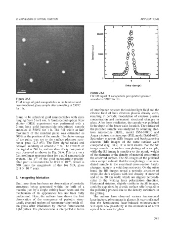
10000
Intensity (a.u.) 5000
0
-1 0 1
Delay time (ps)
Figure 38.6
FWHM signal of nanoparticle precipitated specimen
Figure 38.5 annealed at 550 C for 1 h.
TEM image of gold nanoparticles in the femtosecond
laser-irradiated glass sample after annealing at 550 C
for 1 h.
of interference between the incident light field and the
electric field of bulk electron plasma density wave,
found to be spherical gold nanoparticles with sizes resulting in periodic modulation of electron plasma
ranging from 5 to 8 nm. A femtosecond optical Kerr concentration and permanent structural changes in
shutter (OKS) experiment was performed with a glass. After laser irradiation, the sample was polished
2-mm long gold nanoparticle-precipitated sample to the depth of the beam waist location. The surface of
annealed at 550 C for 1 h. The full width at half the polished sample was analyzed by scanning elec-
maximum of the incident pulse was estimated as tron microscope (JEOL, model JSM-6700F) and
500 fs at the position of the sample. The photo -energy Auger electron spectroscopy (PHI, model SAM-680).
of the pulse was set to the surface plasmon reso- Secondary electron (SE) images and backscattering
nance peak (2.3 eV). The Kerr signal raised and electron (BE) images of the same surface were
decayed suddenly at around t 0. The FWHM of compared (Fig. 38.7). It is well known that the SE
the signal is 240 fs, and no slow decay component image reveals the surface morphology of a sample,
was observed as shown in Fig. 38.6. This is a very while the BE image is sensitive to the atomic weight
fast nonlinear response time for a gold nanoparticle of the elements or the density of material constituting
system. The (3) of the gold nanoparticle-precipi- the observed surface. The SE images of the polished
tated part is estimated to be 0.93 10 –11 , which is silica sample indicate that the morphology of an irra-
300 times the magnitude of that for SiO glass diated sample in the examined cross-section hardly
2
(2.8 10 –14 esu). changes, namely, a void does not exist. On the other
hand, the BE images reveal a periodic structure of
stripe-like dark regions with low density of material
3. Nanograting fabrication and of ca. 20 nm width which are aligned perpendi-
cular to the writing laser polarization direction.
Until now there has been no observation of periodic Horizontal striation, slightly visible in the SE images,
structures being generated within the bulk of a could be explained by a weak surface relief created in
material just by a single writing laser beam and the the polishing process due to the density variations in
mechanism of its appearance has not been fully the grating.
understood. Here, the authors have shown the first The authors have observed various femtosecond
observation of the emergence of periodic struc- laser-induced phenomena in glasses. It was confirmed
turally changed regions of nanometer size inside sil- that the femtosecond laser-induced microstructure
ica glass after irradiation by intense femtosecond will open new possibility in the realization of novel
light pulses. The phenomenon is interpreted in terms optical functions for glass.
581