
Page 80 - Nanotechnology an introduction
P. 80
between the device material and its contact with the external world. Some kinds of transistors depend on the field-dependent barrier arising through
the generation of a space charge (depletion layer) depending on the difference V between the electron Fermi levels of the two materials
b
juxtaposed at the interface and on the sparse presence of carrier-donating impurities (e.g., electron donor centers). The depletion width may be
approximated by
(7.3)
3
16
where N is the impurity concentration, a typical value of which is 10 /cm . Therefore, for silicon, the relative dielectric constant ε of which is 11.9,
W would be about 35 nm for V = 10 mV. Rectification cannot occur if the device is significantly smaller than W, hence the depletion width provides
b
a demarcating length scale below which different behavior occurs.
7.4.3. Single-Electron Devices
Even if the device becomes very small, and at any moment only has one electron passing through it, it does not qualify as a single electron device
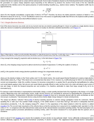
unless the electron is isolated by substantial tunneling barriers to localize its otherwise extended wavefunction, as in Figure 7.9.
Figure 7.9 Single-electron box, consisting of one small semiconductor island separated from a larger electrode (“source”) by a tunnel barrier. An external electric field may be applied to the island using another electrode (the gate)
separated from the small island by a thick insulator preventing tunneling; the field changes the electrochemical potential of the islet, thereby determining the tunneling conditions.
A key concept is the energy E required to add an electron (e.g., to the islet shown in Figure 7.9);
a
(7.4)
where E is the charging energy required to add an electron to an island of capacitance C (=4πε r for a sphere of radius r)
c
0
(7.5)
and E is the quantum kinetic energy (electron quantization energy); for a degenerate electron gas
k
(7.6)
where g is the density of states on the Fermi surface and V is the island volume. One would expect thermal fluctuations to swamp single-electron
effects (SEE) unless E ≥ 10k T. If the island size is somewhat less than about 10 nm, however, E is sufficiently large for SEE to be observable at
a
a
B
normal room temperature. Under this condition, however, E becomes comparable to or greater than E (providing the real justification for calling
k
c
such small islands quantum dots). Not only are such small objects generally difficult to make, but they have to be made with almost exact control of
size and shape, to which the transport properties are very sensitive. It is, therefore, preferable to make them large enough for E not to be
a
dominated by E .
k
For devices in which information is represented as electrostatic charge, a scalar quantity, the lower limit of its magnitude is the charge e of a single
electron. Neglecting noise and equivocation issues, single electron devices can essentially be achieved by downscaling the components of a
conventional transistor. Developments in fabrication technologies (Chapter 8) have led to nanoscale devices with the same architecture as their
microscopic counterparts. Truly nanoscale devices using electrons involve single-charge transport in minute tunnel junctions.
The simple but effective “orthodox” theory [108] of electron tunneling assumes no electron energy quantization inside the conductors. Strictly
speaking this is valid only if the quantum kinetic energy E of the added electron is much less than k T, but seems to adequately describe
B
k
2
observations provided E ≪ E , the charging energy e /C, where C is the capacitance of the object (island) to which the electron is added
k
c
(equation 7.5). The second major assumption of the orthodox theory is that the tunneling time is assumed to be negligibly small—typically it is of the
order of 1 fs—in comparison with other relevant time scales (such as the interval between successive tunneling events). The third assumption is to
ignore coherent quantum processes (simultaneous tunneling events), valid if the barrier resistance R is much greater than the quantum unit of
resistance
(7.7)
which is about 6.5 kΩ. Equation (7.7) ensures the localization of each electron at any particular instant—hence sufficiently nontransparent tunnel
barriers effectively suppress the quantum-mechanical uncertainty of electron location. This suppression makes single-electron manipulation