
Page 84 - Nanotechnology an introduction
P. 84
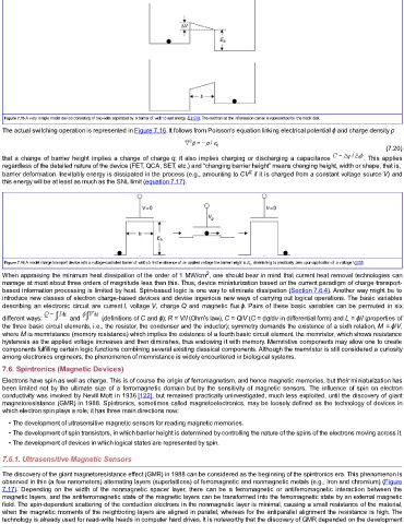
Figure 7.15 A very simple model device consisting of two wells separated by a barrier of width b and energy E b [174]. The electron as the information carrier is represented by the black disk.
  The actual switching operation is represented in Figure 7.16. It follows from Poisson's equation linking electrical potential ϕ and charge density ρ


                                                                                                                      (7.20)
  that a change of barrier height implies a change of charge q; it also implies charging or discharging a capacitance   . This applies
  regardless of the detailed nature of the device (FET, QCA, SET, etc.) and “changing barrier height” means changing height, width or shape; that is,
                                                                            2
  barrier deformation. Inevitably energy is dissipated in the process (e.g., amounting to CV  if it is charged from a constant voltage source V) and
  this energy will be at least as much as the SNL limit (equation 7.17).


  Figure 7.16 A model charge transport device with a voltage-controlled barrier of width b. In the absence of an applied voltage the barrier height is E b , diminishing to practically zero upon application of a voltage V g [32].
                                                               2
  When appraising the minimum heat dissipation of the order of 1 MW/cm , one should bear in mind that current heat removal technologies can
  manage at most about three orders of magnitude less than this. Thus, device miniaturization based on the current paradigm of charge transport-
  based information processing is limited by heat. Spin-based logic is one way to eliminate dissipation (Section 7.6.4). Another way might be to
  introduce new classes of electron charge-based devices and devise ingenious new ways of carrying out logical operations. The basic variables
  describing an electronic circuit are current I,  voltage V,  charge Q  and  magnetic  flux ϕ. Pairs of these basic variables can be permuted in six

  different ways:      and      (definitions of C and ϕ); R = V/I (Ohm's law), C = Q/V (C = dq/dv in differential form) and L = ϕ/I (properties of
  the three basic circuit elements, i.e., the resistor, the condenser and the inductor); symmetry demands the existence of a sixth relation, M = ϕ/V,
  where M is memristance (memory resistance) which implies the existence of a fourth basic circuit element, the memristor, which shows resistance
  hysteresis as the applied voltage increases and then diminshes, thus endowing it with memory. Memristive components may allow one to create
  components fulfilling certain logic functions combining several existing classical components. Although the memristor is still considered a curiosity
  among electronics engineers, the phenomenon of memristance is widely encountered in biological systems.
  7.6. Spintronics (Magnetic Devices)
  Electrons have spin as well as charge. This is of course the origin of ferromagnetism, and hence magnetic memories, but their miniaturization has
  been limited not by the ultimate size of a ferromagnetic domain but by the sensitivity of magnetic sensors. The influence of spin on electron
  conductivity was invoked by Nevill Mott in 1936 [122], but remained practically uninvestigated, much less exploited, until the discovery of giant
  magnetoresistance (GMR) in 1988. Spintronics, sometimes called magnetoelectronics, may be loosely defined as the technology of devices in
  which electron spin plays a role; it has three main directions now:

    • The development of ultrasensitive magnetic sensors for reading magnetic memories.
    • The development of spin transistors, in which barrier height is determined by controlling the nature of the spins of the electrons moving across it.
    • The development of devices in which logical states are represented by spin.

  7.6.1. Ultrasensitive Magnetic Sensors

  The discovery of the giant magnetoresistance effect (GMR) in 1988 can be considered as the beginning of the spintronics era. This phenomenon is
  observed in thin (a few nanometers) alternating layers (superlattices) of ferromagnetic and nonmagnetic metals (e.g., iron and chromium) (Figure
  7.17).  Depending  on  the  width  of  the  nonmagnetic  spacer  layer,  there  can  be  a  ferromagnetic  or  antiferromagnetic  interaction  between  the
  magnetic layers, and the antiferromagnetic state of the magnetic layers can be transformed into the ferromagnetic state by an external magnetic
  field. The spin-dependent scattering of the conduction electrons in the nonmagnetic layer is minimal, causing a small resistance of the material,
  when the magnetic moments of the neighboring layers are aligned in parallel, whereas for the antiparallel alignment the resistance is high. The
  technology is already used for read-write heads in computer hard drives. It is noteworthy that the discovery of GMR depended on the development