Page 85 - Nanotechnology an introduction
P. 85
of methods for making high-quality ultrathin films (Section 6.3.1). The GMR effect has clearly demonstrated that spin-polarized electrons can carry a
  magnetic moment through nonmagnetic materials while maintaining spin coherence: this is the meaning of the term “spin transport” nowadays.


  Figure 7.17 Diagram for describing spin-controlled electron transport in a thin film multilayer. To exploit the giant magnetoresistance effect, layers a and c are ferromagnetic and layer b is a nonmagnetic metal. In the magnetic tunnel
  junction layer b is a dielectric.
  A  second  type  of  magnetic  sensor  is  based  on  the  magnetic  tunnel  junction  (MTJ).  In  this  device,  a  very  thin dielectric  layer  separates
  ferromagnetic (electrode) layers, and electrons tunnel through the nonconducting barrier under the influence of an applied voltage (Figure 7.17). The
  conductivity depends on the relative orientation of the electrode magnetizations and the tunnel magnetoresistance (TMR): it is low for parallel
  alignment of electrode magnetization and high in the opposite case. The magnetic field sensitivity is even greater than for GMR. MTJ devices also
  have high impedance, enabling large signal outputs. In contrast with GMR devices, the electrodes are magnetically independent and can have
  different  critical  fields  for  changing  the  magnetic  moment  orientation.  The  first  laboratory  samples  of  MTJ  structures  (NiFe-Al O -Co)  were
                                                                                                               2 3
  demonstrated in 1995.
  A further direction of development of spintronic devices is based on the development of multilayer structures of ferromagnetic semiconductors,
  which demonstrate properties not available for their metal analogs (e.g., the possibility to control by electric field a magnetic state of material) and
  the giant planar Hall effect, which exceeds by several orders of magnitude the Hall effect in metal ferromagnets. These might be exploited to create
  memory devices, but they have the disadvantages of poor integratability and the necessity of using additional controlling transistors.

  GMR and MTJ are important enablers of size reduction of ferromagnetic memory cells and hence the miniaturization of magnetic random access
  memory  (MRAM),  the  limiting  factor  of  which  is  not  the  ability  to  make  small  ferromagnetic  islands  (which  must  nevertheless  be  above  the
  superparamagnetic size boundary, see Section 2.6) but the ability to sense minute magnetic fields.

  A very important development for increasing storage density is the ability to control the motion of a series of movable domain walls along magnetic
  nanowires by spin-polarized current pulses. This provides the basis of magnetic domain-wall “racetrack” memory.

  7.6.2. Other Memory Devices

  By analogy with ferromagnetic memory, ferroelectric materials are being investigated for nonvolatile storage (nanocapacitor arrays). Using a
  nanoporous  template,  ferroelectric  ceramic  (e.g.,  lead  zirconate  titanate)  can  be  deposited  as  nanoscale  islands  on  a  suitable  metal  (e.g.,
  platinum). They require ultrasensitive electrometers to be read.
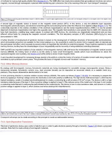
  A more promising direction is resistive random access memory (RRAM). This works as follows (Figure 7.18) [83]. It is necessary to prepare the
  device by applying a “foaming” voltage across the electrodes 2 and 5 (the polarity is indifferent). The high electric field across layer 3, which has the
                                                                                             2
  highest resistance, results in localized electrical breakdown to create a conducting tip a with an area of 10 nm  or less. The device is still in a high
  resistance state because of the layer 4. Now a positive voltage is applied to layer 5. This reduces some of the metal ions in the layer 4 and creates
  a conducting metal filament b continuing the path initiated by the conducting tip. The device is now in a low resistance state, and remains in it until a
  positive voltage is applied to layer 5, which oxidizes and hence destroys the metal filament b.


  Figure 7.18 A resistive random access memory (RRAM) cell. Layer 1 is a silicon substrate, layers 2 and 5 are platinum electrodes, layer 3 is a dielectric oxide (e.g., SiO 2 , Gd 2 O 3 ), 2–20 nm thick; layer 4 is a solid electrolyte (ionic
  conductor), with a resistance about one tenth of that of layer 3, typically a metal-doped nonstoicheometric oxide (with oxygen vacancies) (e.g., MoO 3−x :Cu, 0 ≤ x ≤ 1.5). See text for explanation of operation.
  Crosspoint cell arrays can be made according to this principle to create an addressable memory.

  7.6.3. Spin-Dependent Transistors

  This kind of spintronics device uses control of electron spin in order to gate electrons passing through a transistor. Figure 7.19 shows a proposed
  example. Note that it is made entirely of nonmagnetic materials.

