
Page 83 - Nanotechnology an introduction
P. 83
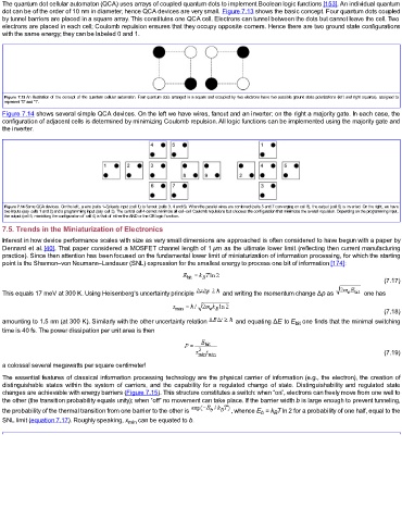
The quantum dot cellular automaton (QCA) uses arrays of coupled quantum dots to implement Boolean logic functions [153]. An individual quantum
  dot can be of the order of 10 nm in diameter, hence QCA devices are very small. Figure 7.13 shows the basic concept. Four quantum dots coupled
  by tunnel barriers are placed in a square array. This constitutes one QCA cell. Electrons can tunnel between the dots but cannot leave the cell. Two
  electrons are placed in each cell; Coulomb repulsion ensures that they occupy opposite corners. Hence there are two ground state configurations
  with the same energy; they can be labeled 0 and 1.


  Figure  7.13 An illustration of the concept of the quantum cellular automaton. Four quantum dots arranged in a square and occupied by two electrons have two possible ground state polarizations (left and right squares), assigned to
  represent “0” and “1”.
  Figure 7.14 shows several simple QCA devices. On the left we have wires, fanout and an inverter; on the right a majority gate. In each case, the
  configuration of adjacent cells is determined by minimizing Coulomb repulsion. All logic functions can be implemented using the majority gate and
  the inverter.


  Figure 7.14 Some QCA devices. On the left, a wire (cells 1–3) leads input (cell 1) to fanout (cells 3, 4 and 6). When the parallel wires are combined (cells 5 and 7 converging on cell 8), the output (cell 9) is inverted. On the right, we have
  two inputs (say cells 1 and 2) and a programming input (say cell 3). The central cell 4 cannot minimize all cell–cell Coulomb repulsions but chooses the configuration that minimizes the overall repulsion. Depending on the programming input,
  the output (cell 5, mimicking the configuration of cell 4) is that of either the AND or the OR logic function.
  7.5. Trends in the Miniaturization of Electronics
  Interest in how device performance scales with size as very small dimensions are approached is often considered to have begun with a paper by
  Dennard et al. [40]. That paper considered a MOSFET channel length of 1 μm as the ultimate lower limit (reflecting then current manufacturing
  practice). Since then attention has been focused on the fundamental lower limit of miniaturization of information processing, for which the starting
  point is the Shannon–von Neumann–Landauer (SNL) expression for the smallest energy to process one bit of information [174]:

                                                                                                                      (7.17)
  This equals 17 meV at 300 K. Using Heisenberg's uncertainty principle    and writing the momentum change Δp as    one has


                                                                                                                      (7.18)
  amounting to 1.5 nm (at 300 K). Similarly with the other uncertainty relation    and equating ΔE to E  one finds that the minimal switching
                                                                                           bit
  time is 40 fs. The power dissipation per unit area is then


                                                                                                                      (7.19)

  a colossal several megawatts per square centimeter!
  The essential features of classical information processing technology are the physical carrier of information (e.g., the electron), the creation of
  distinguishable states within the system of carriers, and the capability for a regulated change of state. Distinguishability and regulated state
  changes are achievable with energy barriers (Figure 7.15). This structure constitutes a switch: when “on”, electrons can freely move from one well to
  the other (the transition probability equals unity); when “off” no movement can take place. If the barrier width b is large enough to prevent tunneling,
  the probability of the thermal transition from one barrier to the other is   , whence E  = k T ln 2 for a probability of one half, equal to the
                                                                                b
                                                                                    B
  SNL limit (equation 7.17). Roughly speaking, x min  can be equated to b.