
Page 82 - Nanotechnology an introduction
P. 82
Localized states with Coulomb interactions cannot have a finite density of states at the Fermi level, which has significant implications for electron
transport within nanoscale material. By definition, at absolute zero all electronic states of a material below the Fermi level are occupied and all
states above it are empty. If an additional electron is introduced, it must settle in the lowest unoccupied state, which is above the Fermi level and
has a higher energy than all the other occupied states. If, on the other hand, an electron is moved from below the Fermi level to the lowest
unoccupied state above it, it leaves behind a positively charged hole, and there will be an attractive potential between the hole and the electron.
2
This lowers the energy of the electron by the Coulomb term −e /(εr) where e is the electron charge, ε the dielectric permittivity, and r the distance
between the two sites. If the density of states at the Fermi level is finite, two states separated by but very close to the Fermi level could be chosen,
2
such that the energy difference was less than e /(εr), which would mean—nonsensically—that the electron in the upper state (above the Fermi level)
has a lower energy than the electron located below the Fermi level. The gap in states that must therefore result is called the Coulomb gap and
materials with a Coulomb gap are called Coulomb glasses.
The single-electron box (Figure 7.9) is unsuitable as a component of an electronic logic device. It has no internal memory; the number of electrons
in it is a unique function of the applied voltage. Furthermore the box cannot carry current; hence a very sensitive electrometer would be needed to
measure its charge state. The latter problem can be overcome by creating a single-electron transistor (Figure 7.11) [108]. Its electrostatic energy is
(cf. equation 7.13)
(7.15)
where n and n are the numbers of electrons passed through the two tunnel barriers. This is the most important single electron device.
2
1
Figure 7.11 Single-electron transistor (cf. Figure 7.9). The hatched areas represent tunneling barriers.
If the source–drain voltage is small no current flows because tunneling would increase the total energy (ΔW < 0 in equation 7.8)—this effect is
called the Coulomb blockade. Simplistically this is because one cannot add less than one electron, hence the flow of current requires a Coulomb
energy of E . The blockade is overcome by a certain threshold voltage V . If one gradually increases the gate voltage V the source–drain
t
c
g
conductance shows sharp resonances almost periodic in V . The quasiperiodic oscillations of the I–V curve are known as Coulomb diamonds and
g
are closely related to the Coulomb staircase.
7.4.4. Molecular Electronic Devices
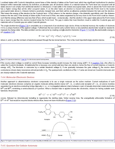
Another approach to ultraminiaturize electronic components is to use a single molecule as the active medium. Current realizations of such
−
+
molecular electronic devices comprise an organic molecule uniting electron donor (D , i.e., a cation) and acceptor (A , i.e., an anion) moieties
separated by an electron-conducting bridge (typically π, i.e., a π-conjugated (alkene) chain) between a pair of (usually dissimilar) metal electrodes
(1)
(2)
M and M , mimicking a semiconductor p–n junction. When a forward bias is applied across the electrodes, chosen for having suitable work
functions, the process
(7.16)
occurs, followed by intramolecular tunneling to regenerate the starting state. Under reverse bias, the energetically unfavorable formation of
2+
2−
D −π−A that would be required blocks electron flow, hence we have rectification (Figure 7.12).
Figure 7.12 A typical molecule (Z-β-(1-hexadecyl-4-quinolinium)-α-cyano-4-styryldicyanomethanide) used to create a rectifying junction (see text). The chemical structure is shown at the top. The energetic structure is shown at the bottom.
7.4.5. Quantum Dot Cellular Automata