
Page 86 - Nanotechnology an introduction
P. 86
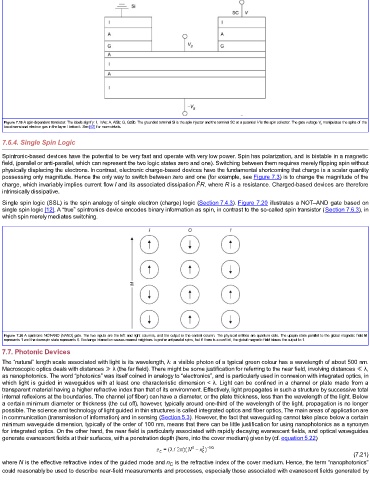
Figure 7.19 A spin-dependent transistor. The labels signify: I, InAs; A, AlSb; G, GaSb. The grounded terminal Si is the spin injector and the terminal SC at a potential V is the spin collector. The gate voltage V g  manipulates the spins of the
  two-dimensional electron gas in the layer I below it. See [67] for more details.

  7.6.4. Single Spin Logic

  Spintronic-based devices have the potential to be very fast and operate with very low power. Spin has polarization, and is bistable in a magnetic
  field, (parallel or anti-parallel, which can represent the two logic states zero and one). Switching between them requires merely flipping spin without
  physically displacing the electrons. In contrast, electronic charge-based devices have the fundamental shortcoming that charge is a scalar quantity
  possessing only magnitude. Hence the only way to switch between zero and one (for example, see Figure 7.3) is to change the magnitude of the
                                                                  2
  charge, which invariably implies current flow I and its associated dissipation I R, where R is a resistance. Charged-based devices are therefore
  intrinsically dissipative.
  Single spin logic (SSL) is the spin analogy of single electron (charge) logic (Section 7.4.3). Figure 7.20 illustrates a NOT–AND gate based on
  single spin logic [12]. A “true” spintronics device encodes binary information as spin, in contrast to the so-called spin transistor (Section 7.6.3), in
  which spin merely mediates switching.


  Figure  7.20 A spintronic NOT-AND (NAND) gate. The two inputs are the left and right columns, and the output is the central column. The physical entities are quantum dots. The upspin state parallel to the global magnetic field M
  represents 1 and the downspin state represents 0. Exchange interaction causes nearest neighbors to prefer antiparallel spins, but if there is a conflict, the global magnetic field biases the output to 1.
  7.7. Photonic Devices
  The “natural” length scale associated with light is its wavelength, λ: a visible photon of a typical green colour has a wavelength of about 500 nm.
  Macroscopic optics deals with distances ≫ λ (the far field). There might be some justification for referring to the near field, involving distances ≪ λ,
  as nanophotonics. The word “photonics” was itself coined in analogy to “electronics”, and is particularly used in connexion with integrated optics, in
  which light is guided in waveguides with at least one characteristic dimension < λ. Light can be confined in a channel or plate made from a
  transparent material having a higher refractive index than that of its environment. Effectively, light propagates in such a structure by successive total
  internal reflexions at the boundaries. The channel (of fiber) can have a diameter, or the plate thickness, less than the wavelength of the light. Below
  a certain minimum diameter or thickness (the cut off), however, typically around one-third of the wavelength of the light, propagation is no longer
  possible. The science and technology of light guided in thin structures is called integrated optics and fiber optics, The main areas of application are
  in communication (transmission of information) and in sensing (Section 5.3). However, the fact that waveguiding cannot take place below a certain
  minimum waveguide dimension, typically of the order of 100 nm, means that there can be little justification for using nanophotonics as a synonym
  for integrated optics. On the other hand, the near field is particularly associated with rapidly decaying evanescent fields, and optical waveguides
  generate evanescent fields at their surfaces, with a penetration depth (here, into the cover medium) given by (cf. equation 5.22)

                                                                                                                      (7.21)
  where N is the effective refractive index of the guided mode and n  is the refractive index of the cover medium. Hence, the term “nanophotonics”
                                                         C
  could reasonably be used to describe near-field measurements and processes, especially those associated with evanescent fields generated by