
Page 312 - Op Amps Design, Applications, and Troubleshooting
P. 312
290 SIGNAL PROCESSING CIRCUITS
FIGURE 7.1 Comparison of silicon and ideal diodes.
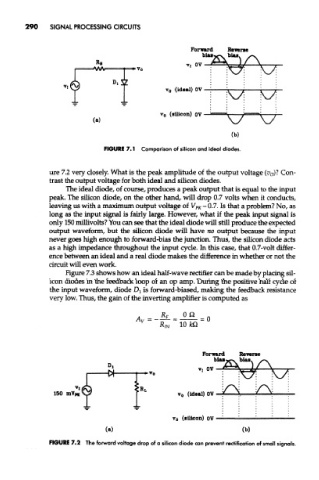
ure 7.2 very closely. What is the peak amplitude of the output voltage (v 0)t Con-
trast the output voltage for both ideal and silicon diodes.
The ideal diode, of course, produces a peak output that is equal to the input
peak. The silicon diode, on the other hand, will drop 0.7 volts when it conducts,
leaving us with a maximum output voltage of V PK - 0.7. Is that a problem? No, as
long as the input signal is fairly large. However, what if the peak input signal is
only 150 millivolts? You can see that the ideal diode will still produce the expected
output waveform, but the silicon diode will have no output because the input
never goes high enough to forward-bias the junction. Thus, the silicon diode acts
as a high impedance throughout the input cycle. In this case, that 0.7-volt differ-
ence between an ideal and a real diode makes the difference in whether or not the
circuit will even work.
Figure 7.3 shows how an ideal half-wave rectifier can be made by placing sil-
icon diodes in the feedback loop of an op amp. During the positive half cycle of
the input waveform, diode DI is forward-biased, making the feedback resistance
very low. Thus, the gain of the inverting amplifier is computed as
FIGURE 7.2 The forward voltage drop of a silicon diode can prevent rectification of small signals.