Page 314 - Op Amps Design, Applications, and Troubleshooting
P. 314
292    SIGNAL PROCESSING CIRCUITS


               one positive and one negative, can be used independently or combined in another
               op amp to produce a full-wave, precision-rectified signal.

        7.2.1 Operation
               Since the op amp in Figure 7.4 is operated with closed-loop negative feedback, the
               inverting (-) input pin is a virtual ground point. Thus, for practical purposes, one
               end of resistors R lf R 2, and R 3 is connected to ground. This means that the total
               input voltage will be developed across RI, causing an input current to flow
               through RI, Since negligible current will flow in or out of the (-) terminal all of the
               input current continues through either R 2 or R 3.
                    On positive input alternations, electron current will leave the output termi-
               nal of the op amp and flow through D lf R 3, and R 1 and out to the positive source.
               Since resistors R t and R 3 are equal values, they will develop equal voltages, so we
               can expect the voltage across R 3 to be the same as the input voltage. Because one
               end of R 3 is grounded, the other end (u 0i) provides a signal equal in amplitude to
               the positive alternation of the input signal. However, because of the direction of
               current flow through R 3, the polarity of the v ol is inverted from v t and produces
               negative half-wave waveforms.
                    During the negative alternation of the input cycle, electron current leaves the
               source and flows through R lf R^ and D 2 and into the output of the op amp. Here
               again, because resistors RI and R 2 have the same current and are equal in value,
               they will have equal voltage drops. Thus, we expect to see a signal at t> 02 that is the
               same amplitude as the input. Additionally, as a result of the direction of the cur-
               rent flow, the t?o2 output will provide a positive half-wave signal.

        7.2.2 Numerical Analysis
               The numerical analysis of the dual, half-wave rectifier circuit shown in Figure 7.4
               is fairly straightforward. We will determine the following characteristics;
                  1. Maximum undipped output signals
                  2. Voltage gain
                  3. Maximum input without distortion
                  4. Highest frequency of operation


               Maximum Output Signal. Outputs v ol and v 02 are one diode drop away
                from the output of the op amp when their respective diode is conducting. There-
                fore, the maximum amplitude that we can expect at outputs v Oi and v m is 0.7 volts
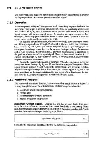
                less than the maximum output of the op amp. That is,


                Similarly, the maximum amplitude for the v O2 output is computed as

