Page 316 - Op Amps Design, Applications, and Troubleshooting
P. 316
294    SIGNAL PROCESSING CIRCUITS


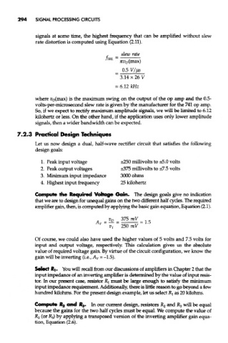
                signals at some time, the highest frequency that can be amplified without slew
                rate distortion is computed using Equation (2.11),


               where v 0(max) is the maximum swing on the output of the op amp and the 0.5-
               voltS'per-microsecond slew rate is given by the manufacturer for the 741 op amp.
               So, if we expect to rectify maximum amplitude signals, we wiM be limited to 6.12
               kilohertz or less. On the other hand, if the application uses only lower amplitude
               signals, then a wider bandwidth can be expected.

        7.2.3 Practical Design Techniques

               Let us now design a dual, half-wave rectifier circuit that satisfies the following
               design goals:

                  1. Peak input voltage           ±250 millivolts to ±5.0 volts
                  2. Peak output voltages         ±375 millivolts to ±7.5 volts
                  3. Minimum input impedance      3000 ohms
                  4. Highest input   frequency    25 kilohertz
               Compute the Required Voltage Gain. The design goals give no indication
               that we are to design for unequal gains on the two different half cycles. The required
               amplifier gain, then, is computed by applying the basic gain equation, Equation (2.1).


               Of course, we could also have used the higher values of 5 volts and 7.5 volte for
               input and output voltage, respectively. This calculation gives us the absolute
               value of required voltage gain. By virtue of the circuit configuration, we know the
               gain will be inverting (i.e., A v = -1.5).

               Select &i. You will recall from our discussions of amplifiers in Chapter 2 that the
               input impedance of an inverting amplifier is determined by the value of input resis-
               tor. In our present case, resistor RI must be large enough to satisfy the minimum
               input impedance requirement. Additionally, there is little reason to go beyond a few
               hundred kilohms. For the present design example, let us select RI as 20 kilohms.

               Compute RI and R 3, In our current design, resistors R 2 and R 3 will be equal
               because the gains for the two half cycles must be equal. We compute the value of
               R 2 (or R 3) by applying a transposed version of the inverting amplifier gain equa-
               tion, Equation (2.6).

