
Page 321 - Op Amps Design, Applications, and Troubleshooting
P. 321
Ideal Biased Clipper 299
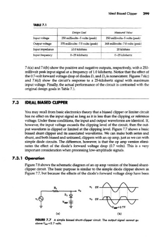
TABU 7.1
Design Goal Measured Value
Input voltage 250 millivolts-5 volts (peak) 250 millivolts-5 volts (peak)
Output voltage 375 millivolts-7.5 volts (peak) 368 millivolts-7.8 volts (peak)
Input impedance >3.0 kilohms 20 kilohms
Input frequency 0-25 kilohertz 0-25 kilohertz
7,6(a) and 7.6(b) show the positive and negative outputs, respectively, with a 250-
millivolt peak input signal at a frequency of 1.0 kilohertz. Notice that the effect of
the 0.7-volt forward voltage drop of diodes D^ and D 2 is nonexistent. Figures 7.6(c)
and 7.6(d) show the circuit's response to a 25-kilohertz signal with maximum
input voltage. Finally, the actual performance of the circuit is contrasted with the
original design goals in Table 7.1.
7.3 IDEAL BIASED CLIPPER
You may recall from basic electronics theory that a biased clipper or limiter circuit
has no effect on the input signal as long as it is less than the clipping or reference
voltage. Under these conditions, the input and output waveforms are identical If,
however, the input voltage exceeds the clipping level of the circuit, then the out-
put waveform is clipped or limited at the clipping level. Figure 7.7 shows a basic
biased shunt clipper and its associated waveforms. We can make both series and
shunt, and both biased and unbiased, clippers with an op amp, just as we can with
simple diode circuits. The difference, however, is that the op amp version elimi-
nates the effect of the diode's forward voltage drop (0.7 volts). This is a very
important consideration when processing low-amplitude signals.
7.3.1 Operation
Figure 7.8 shows the schematic diagram of an op amp version of the biased shunt-
clipper circuit. The basic purpose is similar to the simple diode clipper shown in
Figure 7.7, but because the effects of the diode's forward voltage drop have been
FIGURE 7.7 A simple biased shunt-clipper circuit. The output signal cannot go
above V REF+0.7 volts.