
Page 313 - Op Amps Design, Applications, and Troubleshooting
P. 313
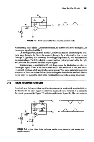
Ideal Rectifier Circuits  291


                           FIGURE 7.3 A half-wave rectifier that simulates an ideal diode.


               Additionally, since diode D 2 is reverse-biased, no current will flow through R 2, so
               the output signal (v 0) will be 0.
                    On the negative half cycle, diode D 2 is forward-biased, completing the feed-
               back loop through R 2. Since the current through R 2 is identical to the current
               through R! {ignoring bias currents), the voltage drop across R 2 will be identical to
               the input voltage. The left end of R 2 is connected to a virtual ground, while the right
               end provides the inverted rectified output signal.
                    It is important to see that the 0.7-volt drop across the diodes has no effect on
               the output signal. Even if the input were only a few tenths of a volt, the circuit
               would still produce a full amplitude output signal. This same principle is applied
               to several of the circuits that follow. By including the diode in the feedback loop of
               the op amp, we make the effects of its nonideal forward voltage drop disappear.


        7.2    IDEAL RECTIFIER CIRCUITS

               Both half- and full-wave ideal rectifier circuits can be made with standard silicon
               diodes and an op amp. Figure 7.4 shows a dual half-wave rectifier. It is similar to
               the circuit presented in Figure 7.3 with the addition of R 3 and R^ The two outputs,


                  FIGURE 7.4 A dual, ideal diode, half-wave rectifier circuit delivering both positive and
                  negative outputs.