
Page 356 - Op Amps Design, Applications, and Troubleshooting
P. 356
334 SIGNAL PROCESSING CIRCUITS
ating level but well below the unity gain frequency of the op amp. The following
equation will provide a reasonable value for C 2.
Substituting values for our present circuit gives us
We will use the nearest standard value of 390 picofarads for C 2.
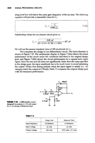
This completes the design of our differentiator circuit. The final schematic is
shown in Figure 7.25. The oscilloscope display in Figure 7.26(a) shows the actual
performance of the circuit under the conditions described in the original design
goal, and Figure 7.26(b) shows the circuit performance for a square-wave input
signal. Since the rise and fall times are significantly faster than the ramp specified
in the design goal, the input amplitude has to be much lower to avoid saturating
the output. Notice that during periods when the input signal is steady (i.e., not
changing states] the output is 0. Finally, Table 7.5 compares the original design goal
with the measured performance.
FIGURE 7.25 A differentiator circuit
designed to produce a ± 10-volt output
for a 16-volt-per-millisecond input.
TABLE 7.5
Design Goal Measured Value
Input frequency 2.0 kilohertz 2.0 kilohertz
Input voltage ±2 volts ±2 volts
Output voltage ±10 volte -10.5 volts, +9.1 volts