Page 424 - Op Amps Design, Applications, and Troubleshooting
P. 424
400    NONIDEAL OP AMP CHARACTERISTICS


                    The negative side, however, is evident in the open-loop frequency response.
               The curve for 3 picofarads does not extend to unity gain (0 dB). That is, we must
               design the circuit to have substantial (e.g., 40-dB) gain to insure stability.

               Feed-Forward Frequency Compensation. The lowest, and therefore most
               dominant, break frequency in an uncompensated op amp is generally caused by
               the frequency response of the PNP transistors in the input stage. Although this
               stage does not provide a voltage gain, the attenuation to the signal increases with
               frequency. By connecting a capacitor between the inverting input and the input of
               the next internal stage, we can effectively bypass the first stage for high frequen-
               cies, thus boosting the overall frequency response of the op amp. This technique is
               called feedforward compensation.
                    The manufacturer must provide access to the input terminal of the second
               stage in order to employ feedforward compensation. In the case of the LM301,
               feedforward compensation is achieved by connecting a capacitor between the
               inverting input and pin 1 (balance). Examination of the internal schematic will
               reveal that this effectively bypasses the NPN differential amplifier on the input
               and the associated level-shifting PNP transistors.
                    When feedforward compensation is used, a small capacitor must be
               employed to bypass the feedback resistor to ensure overall stability. The manufac-
               turer provides details for each op amp that demonstrate the selection of compo-
               nent values.
                    The use of feedforward compensation produces all of the following effects

                  1. Increased small-signal bandwidth
                 2. Increased full-power bandwidth
                 3. Improved slew rate


        10.2.5 Input Resistance

               Calculation of input resistance, or, more correctly, input impedance, was pre-
               sented in Chapter 2. In the case of a noninverting configuration, we found that the
               open-loop input resistance of the op amp is magnified when the feedback loop is
               closed. Equation (2.29) is used to determine the effective input impedance once
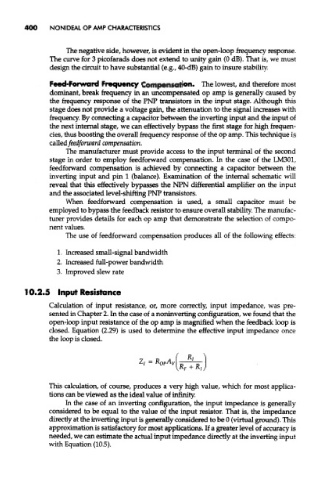
               the loop is closed.


               This calculation, of course, produces a very high value, which for most applica-
               tions can be viewed as the ideal value of infinity.
                    In the case of an inverting configuration, the input impedance is generally
               considered to be equal to the value of the input resistor. That is, the impedance
               directly at the inverting input is generally considered to be 0 (virtual ground). This
               approximation is satisfactory for most applications. If a greater level of accuracy is
               needed, we can estimate the actual input impedance directly at the inverting input
               with Equation (10.5).

