
Page 425 - Op Amps Design, Applications, and Troubleshooting
P. 425
Summary and Recommendations 401
The total input impedance for the amplifier circuit is simply the sum of the input
resistor and the value computed with Equation (10.5).
10.2.6 Output Resistance
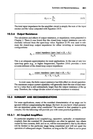
The calculation and effects of output resistance, or impedance, were presented in
Chapter 2. There it was found that the closed-loop output resistance was sub-
stantially reduced from the open-loop value. Equation (2.15) was used to esti-
mate the closed-loop output impedance for either inverting or noninverting
configurations:
This is an adequate approximation for most applications. In the case of very low
open-loop gains (e.g., at higher frequencies), Equation (10.6) provides a more
accurate estimate of the closed-loop output impedance.
In most cases, the finite output resistance has little effect on circuit operation.
The maximum output current capability will generally limit the size of load resis-
tor to a value that is still substantially larger than the output resistance of the op
amp. Therefore, the voltage divider action of output resistance is minimal.
10.3 SUMMARY AND RECOMMENDATIONS
For some applications, many of the nonideal characteristics of op amps can be
ignored without compromising the design. But how do you know which parame-
ters are important under what conditions? The answer to that question is quite
complex, but the following will provide you with some practical guidelines.
10.3.1 AC-Coupled Amplifiers
If a particular amplifier is AC-coupled (e.g., capacitive-, optically-, or transformer-
coupled), then the nonideal DC characteristics can often be ignored. Any offsets
caused by bias currents, drift, and so on, will be noncumulative; mat is, the effects
will be limited to the particular stage being considered and will not upset the
operation of subsequent stages. Therefore, as long as the DC offset is not so great