
Page 59 - Op Amps Design, Applications, and Troubleshooting
P. 59
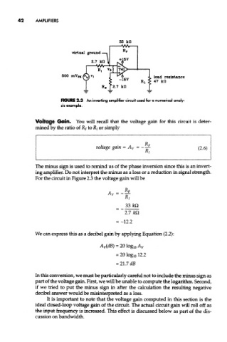
42     AMPLIFIERS


                          FIGURE 2.3 An inverting amplifier circuit used for a numerical analy-
                          sis example.


               Voltage Gain. You will recall that the voltage gain for this circuit is deter-
               mined by the ratio of JR f to R { or simply


               The minus sign is used to remind us of the phase inversion since this is an invert-
               ing amplifier. Do not interpret the minus as a loss or a reduction in signal strength.
               For the circuit in Figure 2.3 the voltage gain will be

                                             A -   *F


               We can express this as a decibel gain by applying Equation (2.2):


               In this conversion, we must be particularly careful not to include the minus sign as
               part of the voltage gain. First, we will be unable to compute the logarithm. Second,
               if we tried to put the minus sign in after the calculation the resulting negative
               decibel answer would be misinterpreted as a loss.
                    It is important to note that the voltage gain computed in this section is the
               ideal closed-loop voltage gain of the circuit. The actual circuit gain will roE off as
               the input frequency is increased. This effect is discussed below as part of the dis-
               cussion on bandwidth.