
Page 106 - Optofluidics Fundamentals, Devices, and Applications
P. 106
Optofluidic Trapping and Transport Using Planar Photonic Devices 87
5-3-2 A Detailed Example—Optofluidic Transport in PDMS
Microfluidics Using SU-8 Waveguides
As mentioned earlier our goal in this section is not only to review
the literature but also to provide the reader with sufficient informa-
tion to exploit optofluidic transport within microfluidic devices of
their own design. The technique we presented in this section is
based on that presented by Schmidt et al. [49] and uses SU-8 wave-
guides with PDMS microfluidics. We choose to present this in detail
here because of the relative ease with which both these types of
devices can be manufactured.
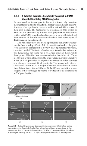
The basic layout of our basic optofluidic transport architec-
ture is shown in Fig. 5-5a to 5-5c. As mentioned earlier, the plat-
form used here comprises SU-8 epoxy-based photonic structures,
combined with PDMS microfluidics on a fused silica substrate.
The fused silica substrate has a refractive index of 1.453, while
the exposed SU-8 film has a measured refractive index of 1.554 at
λ= 975 nm which, along with the water cladding with refractive
index of 1.33, provides for significant refractive index contrast
and strong evanescent field gradients. The waveguide dimen-
sions were chosen to be a height of 560 nm and varied in width
from 2.8 μm to as little as 500 nm. At the 975-nm excitation wave-
length all these waveguide widths were found to be single mode
in TM polarization.
Fluid Particle Waveguide
flow
Optical transport
2 μm
Waveguide
Waveguide input
(b) (c)
(a)
Particle Particle Particle
Flow
975-nm
light
Waveguide
(d) (e) (f)
FIGURE 5-5 Optical trapping and transport in the evanescent fi eld of an optical
waveguide. (a,b) A particle fl owing in a microchannel becomes captured in the
evanescent fi eld of the excited waveguide. (c) SEM of two waveguides. (d–f) Time
step images showing transport of 3-μm polystyrene particles on a waveguide.