
Page 289 - Optofluidics Fundamentals, Devices, and Applications
P. 289
Optofluidic Micr oscope 263
Specimen
Illumination
PDMS
channel
Apertures
CMOS
Al layer Flow (b) OFM imaging
(a)
Channel Cross
Y v <50%
X correlation
Screen out
Specimen >50%
>50%
1 μm
L = 9.9 μm Automatic
ΔX θ measurement
δY = 500 nm
(c) (d)
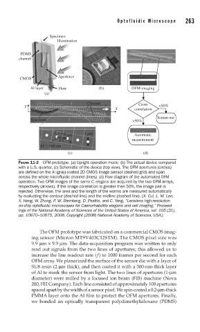
FIGURE 11-2 OFM prototype. (a) Upright operation mode. (b) The actual device compared
with a U.S. quarter. (c) Schematic of the device (top view). The OFM apertures (circles)
are defi ned on the Al (gray)-coated 2D CMOS image sensor (dashed grid) and span
across the whole microfl uidic channel (lines). (d) Flow diagram of the automated OFM
operation. Two OFM images of the same C. elegans are acquired by the two OFM arrays,
respectively (arrows). If the image correlation is greater then 50%, the image pair is
rejected. Otherwise, the area and the length of the worms are measured automatically
by evaluating the contour (dashed line) and the midline (dashed line). (X. Cui, L. M. Lee,
X. Heng, W. Zhong, P. W. Sternberg, D. Psaltis, and C. Yang, “Lensless high-resolution
on-chip optofl uidic microscopes for Caenorhabditis elegans and cell imaging,” Proceed-
ings of the National Academy of Sciences of the United States of America, vol. 105 (31),
pp. 10670–10675, 2008. Copyright (2008) National Academy of Sciences, USA.)
The OFM prototype was fabricated on a commercial CMOS imag-
ing sensor (Micron MT9V403C12STM). The CMOS pixel size was
9.9 μm × 9.9 μm. The data-acquisition program was written to only
read out signals from the two lines of apertures; this allowed us to
increase the line readout rate ( f) to 1000 frames per second for each
OFM array. We planarized the surface of the sensor die with a layer of
SU8 resin (2 μm thick), and then coated it with a 300-nm-thick layer
of Al to mask the sensor from light. The two lines of apertures (1-μm
diameter) were milled by a focused ion beam (FIB) machine (Nova
200, FEI Company). Each line consisted of approximately 100 apertures
spaced apart by the width of a sensor pixel. We spin-coated a 0.2-μm-thick
PMMA layer onto the Al film to protect the OFM apertures. Finally,
we bonded an optically transparent polydimethylsiloxane (PDMS)