
Page 132 - Organic Electronics in Sensors and Biotechnology
P. 132
Strain and Pressure Sensors Based on OFET 109
4. The sensor transduction bandwidth should not be less than
100 Hz, intended as tactile image frame frequency. Individual
sensing units should accordingly possess a faster response,
related to their number, when multiplexing is performed.
5. Spatial resolution should be at least of the order of 1 to 2 mm,
as a reasonable compromise between gross grasping and fine
manipulation tasks.
The development of tactile sensors is one of the most difficult
aspects of robotics. Many technologies have been explored, includ-
ing a carbon-loaded elastomer, piezoelectric materials, and micro-
electromechanical systems. Artificial skin examples, able to detect
pressure, already exist; but it is difficult to manufacture artificial
skin in large enough quantities to cover a robot body, and it does
not stretch. The most promising examples of “electronic skin-like”
systems with large areas are based on organic semiconductors and
have been reported by Takao Someya’s group at University of
Tokyo. They have developed conformable, flexible, wide-area net-
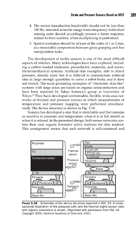
24
works of thermal and pressure sensors in which measurements of
temperature and pressure mapping were performed simultane-
ously. The device structure is shown in Fig. 3.18.
Someya has developed a skin that is stretchable and that remains
as sensitive to pressure and temperature when it is at full stretch as
when it is relaxed. In the presented design, both sensor networks con-
tain their own organic transistor active matrices for data readout.
This arrangement means that each network is self-contained and
Polyimide Pen
Anode
Cu Thermal CuPc (P)
sensor PTCDI (N)
Conductive rubber Cathode
Pressure Parylene
sensor
Au
Paste
Au Au
Parylene Parylene
s Pentacene d s Pentacene d
Polyimide Transistor Polyimide
g g
Base film Base film
FIGURE 3.18 Schematic of the device structure reported in Ref. 24. A cross-
sectional illustration of the pressure (left) and the thermal (right) sensor cells
with organic transistors is shown. (Reprinted with permission from Ref. 24.
Copyright 2005, National Academy of Sciences, USA.)