
Page 129 - Organic Electronics in Sensors and Biotechnology
P. 129
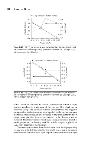
106    Cha pte r  T h ree

                                  Top contact  Bottom contact

                            0.1                          –0.1
                          ΔV th /V th  (bottom)  –0.1    –0.1  ΔV th /V th  (top)
                                                         –0.0
                            0.0

                           –0.2
                                                         –0.2
                           –0.3
                                                         –0.4
                           –0.4                          –0.3
                               –2  0 2 4 6 8  10 12 14 16 18 20
                                       Pressure (kPa)
               FIGURE 3.14  ΔV /V  vs. pressure for a bottom-contact device (left axis) and
                            t   t 0
               for a top-contact device (right axis). (Reprinted from Ref. 16. Copyright 2007,
               with permission from Elsevier.)


                                  Top contact  Bottom contact
                            0.0                             0.0
                           –0.2                            –0.2
                         Δμ/μ 0 (top)  –0.4                –0.4 Δμ/μ 0 (bottom)

                           –0.6
                                                           –0.6
                           –0.8                            –0.8
                           –1.0                            –1.0

                              –2 0 2  4 6 8 10 12 14 16 18 20
                                       Pressure (kPa)

               FIGURE 3.15  Δμ/μ  vs. pressure for a bottom-contact device (left axis) and
                              0
               for a top-contact device (right axis). (Reprinted from Ref. 16. Copyright 2007,
               with permission from Elsevier.)

               of the current of the FETs. In contrast, tensile strain causes a larger
               spacing, resulting in a decrease of the current. This effect can be
               observed in Fig. 3.16 in which positive (tensile strain) and negative
               (compressive strain) pressures were applied to the device. As seen,
               the tensile stimulus results in a decrease of the drain current while a
               compressive stimulus induces an increase in the drain current as
               expected. This feature cannot be achieved using commercial (metallic)
               strain gauges and can be very useful in a wide range of applications
               (e.g., body parameters monitoring).
                   The main drawbacks of these devices seem to be the high operating
               voltage and a limited time stability that could be overcome by using a
               proper flexible encapsulation layer to protect the semiconductor layer