
Page 125 - Organic Electronics in Sensors and Biotechnology
P. 125
102 Cha pte r T h ree
3.3.2 Substrate-Free Organic Thin-Film Strain
and Pressure Sensors
In this section we describe organic semiconductor field-effect
mechanical sensors based on a substrate-free OTFT structure. Papers
regarding this kind of sensor have already been published by us. 15–17
The proposed device is completely flexible and combines both
switching and sensing functions. These are very interesting hall-
marks since there are only a few examples of organic mechanical
sensors reported in the literature, as shown in the previous section,
and none of them exploits all the advantages of organic devices.
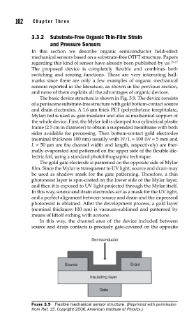
The basic device structure is shown in Fig. 3.9. The device consists
of a pentacene substrate-free structure with gold bottom-contact source
and drain electrodes. A 1.6 μm thick PET (polyethylene terephtalate,
Mylar) foil is used as gate insulator and also as mechanical support of
the whole device. First, the Mylar foil is clamped to a cylindrical plastic
frame (2.5 cm in diameter) to obtain a suspended membrane with both
sides available for processing. Then bottom-contact gold electrodes
(nominal thickness 100 nm) usually with W/L = 100 (W = 5 mm and
L = 50 μm are the channel width and length, respectively) are ther-
mally evaporated and patterned on the upper side of the flexible die-
lectric foil, using a standard photolithographic technique.
The gold gate electrode is patterned on the opposite side of Mylar
film. Since the Mylar is transparent to UV light, source and drain may
be used as shadow mask for the gate patterning. Therefore, a thin
photoresist layer is spin-coated on the lower side of the Mylar layer,
and then it is exposed to UV light projected through the Mylar itself.
In this way, source and drain electrodes act as a mask for the UV light,
and a perfect alignment between source and drain and the impressed
photoresist is obtained. After the development process, a gold layer
(nominal thickness 100 nm) is vacuum-sublimed and patterned by
means of liftoff etching with acetone.
In this way, the channel area of the device included between
source and drain contacts is precisely gate-covered on the opposite
Semiconductor
Source Drain
Insulating layer
Gate
FIGURE 3.9 Flexible mechanical sensor structure. (Reprinted with permission
from Ref. 15. Copyright 2006, American Institute of Physics.)