
Page 120 - Organic Electronics in Sensors and Biotechnology
P. 120
Strain and Pressure Sensors Based on OFET 97
g
s d
FIGURE 3.2 Equivalent circuit diagram of the device. (Reprinted with permission
from Ref. 7. Copyright 2003 IEEE.)
organic transistors are used to address the rubber pressure-sensitive
elements in a sensor array. The equivalent circuit diagram is shown in
Fig. 3.2.
8
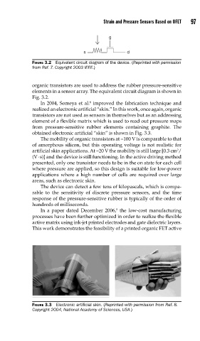
In 2004, Someya et al. improved the fabrication technique and
realized an electronic artificial “skin.” In this work, once again, organic
transistors are not used as sensors in themselves but as an addressing
element of a flexible matrix which is used to read out pressure maps
from pressure-sensitive rubber elements containing graphite. The
obtained electronic artificial “skin” is shown in Fig. 3.3.
The mobility of organic transistors at −100 V is comparable to that
of amorphous silicon, but this operating voltage is not realistic for
2
artificial skin applications. At −20 V the mobility is still large [0.3 cm /
(V · s)] and the device is still functioning. In the active driving method
presented, only one transistor needs to be in the on state for each cell
where pressure are applied, so this design is suitable for low-power
applications where a high number of cells are required over large
areas, such as electronic skin.
The device can detect a few tens of kilopascals, which is compa-
rable to the sensitivity of discrete pressure sensors, and the time
response of the pressure-sensitive rubber is typically of the order of
hundreds of milliseconds.
9
In a paper dated December 2006, the low-cost manufacturing
processes have been further optimized in order to realize the flexible
active matrix using ink-jet printed electrodes and gate dielectric layers.
This work demonstrates the feasibility of a printed organic FET active
FIGURE 3.3 Electronic artifi cial skin. (Reprinted with permission from Ref. 8.
Copyright 2004, National Academy of Sciences, USA.)