
Page 121 - Organic Electronics in Sensors and Biotechnology
P. 121
98 Cha pte r T h ree
PEN film
• Cu electrode
Pressure-sensitive rubber
Au pad
V dd Parylene
d Pentacene s Via hole
BL Polyimide
Gate (WL)
Polyimide film
Epoxy partition
Pressure-
sensitive
rubber
Cu
FET
1 cm
Word-line Epoxy (d)
partition BL
Gate Pentacene FET
V WL WL
Drain
Pressure-
sensitive
rubber
Source
Bit-line 1 mm
V dd
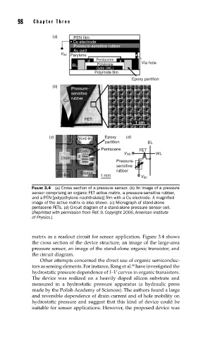
FIGURE 3.4 (a) Cross section of a pressure sensor. (b) An image of a pressure
sensor comprising an organic FET active matrix, a pressure-sensitive rubber,
and a PEN [poly(ethylene naphthalate)] fi lm with a Cu electrode. A magnifi ed
image of the active matrix is also shown. (c) Micrograph of stand-alone
pentacene FETs. (d) Circuit diagram of a stand-alone pressure sensor cell.
(Reprinted with permission from Ref. 9. Copyright 2006, American Institute
of Physics.)
matrix as a readout circuit for sensor application. Figure 3.4 shows
the cross section of the device structure, an image of the large-area
pressure sensor, an image of the stand-alone organic transistor, and
the circuit diagram.
Other attempts concerned the direct use of organic semiconduc-
10
tors as sensing elements. For instance, Rang et al. have investigated the
hydrostatic pressure dependence of I–V curves in organic transistors.
The device was realized on a heavily doped silicon substrate and
measured in a hydrostatic pressure apparatus (a hydraulic press
made by the Polish Academy of Sciences). The authors found a large
and reversible dependence of drain current and of hole mobility on
hydrostatic pressure and suggest that this kind of device could be
suitable for sensor applications. However, the proposed device was