
Page 126 - Organic Electronics in Sensors and Biotechnology
P. 126
Strain and Pressure Sensors Based on OFET 103
part of the insulator (see Fig. 3.9), thus limiting all the parasitic capac-
itance effects due to source-drain and gate metal overlapping. 18
Residual hysteresis can be interpreted both in terms of border effects
and with trapping charge effects in the semiconductor. 19–21
The marked sensitivity of the drain current to an elastic deforma-
tion induced by a mechanical stimulus, and the fact that the device is
so thin and flexible that it can be applied to whatever surface, can be
exploited to detect through the variation of the channel current any
mechanical deformation of the surface itself. In particular, we investi-
gated the sensitivity of the device to a pressurized airflow applied on
the gate side of the suspended membrane and the sensitivity to a
strain or a bending imposed by a deformation of the device.
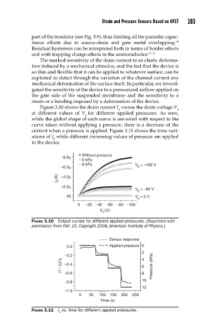
Figure 3.10 shows the drain current I versus the drain voltage V
d d
at different values of V for different applied pressures. As seen,
g
while the global shape of each curve is unvaried with respect to the
curve taken without applying a pressure, there is a decrease of the
current when a pressure is applied. Figure 3.11 shows the time vari-
ations of I while different increasing values of pressure are applied
d
to the device.
–8.0μ Without pressure
6 kPa
–6.0μ 9 kPa V g = –100 V
I d (A) –4.0μ
–2.0μ
V g = –60 V
00 V g = 0 V
0 –20 –40 –60 –80 –100
V d (V)
FIGURE 3.10 Output curves for different applied pressures. (Reprinted with
permission from Ref. 15. Copyright 2006, American Institute of Physics.)
Sensor response
0.0 Applied pressure 0
2
–0.2
I 0 )/I 0 –0.4 4
– 6 Pressure (kPa)
(I –0.6 8
10
–0.8
12
–1.0
0 50 100 150 200 250
Time (s)
FIGURE 3.11 I vs. time for different applied pressures.
d