
Page 124 - Organic Electronics in Sensors and Biotechnology
P. 124
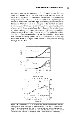
Strain and Pressure Sensors Based on OFET   101

               pentacene film was vacuum-sublimed, and finally 60 nm thick Au
               drain and source electrodes were evaporated through a shadow
               mask. For comparison a capacitor was also manufactured simultane-
               ously in the same base film. The authors observed large changes in
               the drain current that cannot be explained only by the deformation of
               the device structure. Then in the analysis of the electrical character-
               istics, changes in the structural parameters of the transistors (namely,
               channel width W and length L and the thickness of the gate insulator)
               were taken into account to evaluate possible variations in the mobility
               of the transistor. The transfer characteristics of the realized transistor
               and the mobility variations observed are shown in Fig. 3.8 as a func-
               tion of strain or bending radius. The mobility increases monotonically
               when the strain is changed from tension to compression passing
               through the flat state.


                            –15                         4.6
                                 (a)                    8.1
                                                        17
                            –10
                           I ds (μA)  –5  Compression  R (mm)


                              0
                                                       17
                                 (b)                   10.5
                           I ds (μA)  –10  Tension      5.9
                                                        4.6
                             –5
                                                     R (mm)
                              0
                               20  10  0  –10 –20 –30 –40 –50
                                              (V)
                                           V gs
                                      Bending radii (mm)
                                   4 5 6 10  30  30  10  6 5  4
                              1.2                         1.2
                                  (c)         (d )
                              1.1                         1.1
                            μ/μ 0  1.0                    1.0  μ/μ 0


                              0.9                         0.9
                                    Tension     Compression
                              0.8                         0.8
                                –2 –1.5  –1 –0.5  0 0.5  1 1.5  2
                                          Strain (%)

               FIGURE 3.8  Transfer curves on (a) compressive and (b) tensile strains. Mobility
               as function of strain or bending radius in (c) tensile strain and (d) compressive
                    14
               strain.  Solid and open circles refer to transistors whose source-drain current
               path is, respectively, parallel and perpendicular to the strain direction. (Reprinted
               with permission from Ref. 14. Copyright 2005, American Institute of Physics.)