
Page 122 - Organic Electronics in Sensors and Biotechnology
P. 122
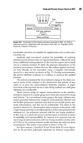
Strain and Pressure Sensors Based on OFET   99


                                                    PVA
                                                      Pentacene


                            Source                    Drain
                                     PVP gate dielectric
                                         Gate
                                     Glass substrate

               FIGURE 3.5  Schematic of the device structure reported in Ref. 11; PVA is
               poly(vinyl alcohol). (Reprinted with permission from Ref. 11. Copyright 2005,
               American Institute of Physics.)

               not flexible, therefore not suitable for applications such as robot skin,
               e-textiles, etc.
                                        11
                   Darlinski and coworkers  studied the possibility of realizing
               pressure sensors based solely on organic transistors, without the need
               of any additional sensing element. In this way the organic device itself
               acts as a sensing element. To study the pressure dependence of the
               electrical performance of these devices, the authors applied mechani-
               cal force directly on the transistors using a tungsten microneedle
               moved by a step motor, as shown in Fig. 3.5. During measurements,
               the device substrate is placed on a balance to measure the applied
               pressure.
                   The authors explained the force-induced change in the drain cur-
               rent in terms of the variation in the distribution and activity of trap
               states at or near the semiconductor/dielectric interface.  A major
               drawback of the reported device is that, being realized on a stiff glass
               substrate, it is not flexible.
                   Strain sensors using an organic semiconductor as the sensitive
               (resistive) element of a strain gauge have been also reported by Jung
               and Jackson.  In conventional strain gauges, the large stiffness mis-
                          12
               match generated between the inorganic semiconductor element and
               the flexible (polymeric) substrate may lead to irreversible plastic sub-
               strate deformations, and this can be problematic. The stress in the
               sensitive element (i.e., the inorganic semiconductor or the metal, with
               a high Young modulus) is not representative of the stress present in the
               substrate (i.e., the polymeric material with the low Young modulus).
               In this way, as a result, the sensor’s performance is reduced in terms
               of reliability and reproducibility. In contrast, it is expected that the
               use of organic semiconductors with low Young modulus (on the order
               of 5 GPa) as the sensing element would minimize the induced stress
               concentration. The sensor cross section is shown in Fig. 3.6.
                   For these sensors, 2 nm thick Ti and 20 nm thick Au were depos-
               ited on 50  μm thick polyimide substrates by thermal evaporation.