
Page 127 - Organic Electronics in Sensors and Biotechnology
P. 127
104 Cha pte r T h ree
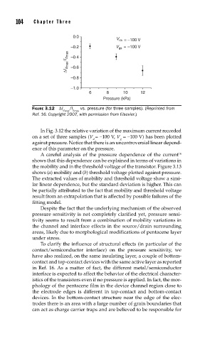
0.0
V ds = –100 V
–0.2 V gs = –100 V
ΔI d max /I d max –0.4
–0.6
–0.8
–1.0
6 8 10 12
Pressure (kPa)
FIGURE 3.12 ΔI /I vs. pressure (for three samples). (Reprinted from
d max d max
Ref. 16. Copyright 2007, with permission from Elsevier.)
In Fig. 3.12 the relative variation of the maximum current recorded
on a set of three samples (V =−100 V, V =−100 V) has been plotted
d g
against pressure. Notice that there is an uncontroversial linear depend-
ence of this parameter on the pressure.
A careful analysis of the pressure dependence of the current 16
shows that this dependence can be explained in terms of variations in
the mobility and in the threshold voltage of the transistor. Figure 3.13
shows (a) mobility and (b) threshold voltage plotted against pressure.
The extracted values of mobility and threshold voltage show a simi-
lar linear dependence, but the standard deviation is higher. This can
be partially attributed to the fact that mobility and threshold voltage
result from an extrapolation that is affected by possible failures of the
fitting model.
Despite the fact that the underlying mechanism of the observed
pressure sensitivity is not completely clarified yet, pressure sensi-
tivity seems to result from a combination of mobility variations in
the channel and interface effects in the source/drain surrounding
areas, likely due to morphological modifications of pentacene layer
under stress.
To clarify the influence of structural effects (in particular of the
contact/semiconductor interface) on the pressure sensitivity, we
have also realized, on the same insulating layer, a couple of bottom-
contact and top-contact devices with the same active layer as reported
in Ref. 16. As a matter of fact, the different metal/semiconductor
interface is expected to affect the behavior of the electrical character-
istics of the transistors even if no pressure is applied. In fact, the mor-
phology of the pentacene film in the device channel region close to
the electrode edges is different in top-contact and bottom-contact
devices. In the bottom-contact structure near the edge of the elec-
trodes there is an area with a large number of grain boundaries that
can act as charge carrier traps and are believed to be responsible for