
Page 123 - Organic Electronics in Sensors and Biotechnology
P. 123
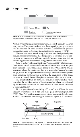
100    Cha pte r  T h ree


                               Kapton (50 μm)   Au

                               Titanium         p-doped pentacene
               FIGURE 3.6  Cross section of the organic semiconductor strain sensor.
               (Reprinted with permission from Ref. 12. Copyright 2003, IEEE.)

               Next, a 50 nm thick pentacene layer was deposited, again by thermal
               evaporation. The pentacene layer was then doped p-type by exposure
               to a 1% solution of ferric chloride in water. The maximum process
               temperature used to fabricate the organic strain sensors is 110°C.
                   The devices were tested using a Wheatstone bridge configura-
               tion, and the results indicate that it is possible to fabricate at low tem-
               perature a strain sensor with mechanical characteristics matched to
               low-Young-modulus substrates using organic semiconductors.
                                                13
                   Jung et al. have also demonstrated  the possibility of combining
               these sensors with pentacene-based thin-film transistors as temper-
               ature sensors. The strain sensor consists of a Wheatstone bridge
               structure where the pentacene film acts as sensing layer of a strain
               gauge, while the temperature sensors adopt a bottom-contact penta-
               cene transistor configuration in which the variations of the drain
               currents in the subthreshold regime are measured vs. temperature.
                   The effects of strain on pentacene transistor characteristics while
               changing the bending radius of the structure have been investigated
               by Sekitani and coworkers.  A cross section of their device structure
                                      14
               is shown in Fig. 3.7.
                   First, a gate electrode consisting of 5 nm Cr and 100 nm Au was
               vacuum-evaporated on a 125  μm thick poly-ethylenenaphthalate
               (PEN) film. Polyimide precursors were then spin-coated and cured
               at 180°C to form 900 nm thick gate dielectric layers. A 50 nm thick


                                     FET               Capacitor
                         Au(s)                Au(d)
                                  Pentacene                   Au


                                           Base film (PEN)

                        Polyimide   Au(g)                   Au
               FIGURE 3.7  Cross section of the organic FET and capacitor reported in Ref. 14.
               (Reprinted with permission from Ref. 14. Copyright 2005, American Institute of
               Physics.)