
Page 119 - Organic Electronics in Sensors and Biotechnology
P. 119
96 Cha pte r T h ree
3.3 Strain and Pressure Sensors
The effect of strain on the mechanical and electronic properties of
organic semiconductors is an emerging research topic in fundamen-
tal physics and applications. Although mechanical flexibility is one of
the main advantages of organic materials, relatively little progress
has been made in the field of pressure or bending recognition mainly
because mechanical sensing requires attributes of conformability and
flexibility and three-dimensional large-area shaping that in many
cases are difficult to achieve even for organic devices.
On the other hand, in the application domain, artificial sense of
touch is considered an essential feature of future generations of
robots, and wearable electronics has become one of the hottest themes
in electronics, aiming at the design and production of a new genera-
tion of garments with distributed sensors and electronic functions.
3.3.1 State of the Art in Strain and Pressure Sensors
Based on Organic Materials
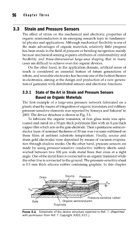
The first example of a large-area pressure network fabricated on a
plastic sheet by means of integration of organic transistors and rubbery
7
pressure-sensitive elements was reported by Someya and Sakurai in
2003. The device structure is shown in Fig. 3.1.
To fabricate the organic transistor, at first glass resin was spin-
coated and cured on a 50 μm thick polyimide film with an 8 μm thick
copper film which acts as the gate electrode. Then a pentacene semicon-
ductor layer of nominal thickness of 30 nm was vacuum-sublimed on
these films at ambient substrate temperature. Finally, source and
drain gold electrodes were deposited by means of vacuum evapora-
tion through shadow masks. On the other hand, pressure sensors are
made by using pressure-sensitive conductive rubbery sheets sand-
wiched between two 100 μm wide metal lines that cross at a right
angle. One of the metal lines is connected to an organic transistor while
the other line is connected to the ground. The pressure-sensitive sheet
is 0.5 mm thick silicone rubber containing graphite. In this chapter
Source
Drain Pressure
Plastic sheet V ss
V dd
Pressure-sensitive rubber
Gate Organic semiconductor
Polyimide
FIGURE 3.1 Schematic of the device structure reported in Ref. 7. (Reprinted
with permission from Ref. 7. Copyright 2003, IEEE.)