Page 149 - Organic Electronics in Sensors and Biotechnology
P. 149

126    Cha pte r  F o u r

                                100
                                90
                                        V 1
                               Layer voltage/bias voltage (%)  50  tot
                                80
                                        V
               C 1  C 2  C 3    70      V V 2 3
                                60
            R c
               R 1  R 2  R 3    40
                                30
                                20
                                10
                                 0
                                 1.E–06   1.E–04  1.E–02   1.E+00   1.E+02
                                                  Time (s)
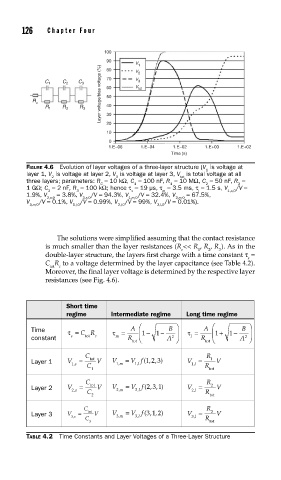
          FIGURE 4.6  Evolution of layer voltages of a three-layer structure (V  is voltage at
                                                            1
          layer 1, V  is voltage at layer 2, V  is voltage at layer 3, V  is total voltage at all
                                   3
                 2
                                                    tot
          three layers; parameters: R = 10 kΩ, C = 100 nF, R = 10 MΩ, C = 50 nF, R =
                               C        1         1        2        2
          1 GΩ; C = 2 nF, R = 100 kΩ; hence τ = 19 μs, τ = 3.5 ms, τ = 1.5 s, V  /V =
                3       3              s        m        l       1,s,0
          1.9%, V  = 3.8%, V  /V = 94.3%, V  /V = 32.4%, V  = 67.5%,
                2,s,0     3,s,0       1,m,0        2,m,0
          V   /V = 0.1%, V  /V = 0.99%, V  /V = 99%, V  /V = 0.01%).
           3,m,0       1,l,0       2,l,0      3,l,0
                   The solutions were simplified assuming that the contact resistance
               is much smaller than the layer resistances (R << R , R , R ). As in the
                                                     c   1  2  3
               double-layer structure, the layers first charge with a time constant τ  =
                                                                       s
               C R  to a voltage determined by the layer capacitance (see Table 4.2).
                 tot  c
               Moreover, the final layer voltage is determined by the respective layer
               resistances (see Fig. 4.6).
                     Short time
                     regime      Intermediate regime  Long time regime
                                         ⎛       B ⎞         ⎛       B ⎞
            Time      τ =  CR     τ =  A  ⎜ 1  − 1 −  ⎟  τ =  A  ⎜ 1 + 1  −  ⎟
                                                                      2
                                                  2
            constant  s   tot  c   m  R  ⎝       A ⎠   l  R  ⎝       A ⎠
                                       tot                 tot
                          C                                 R
                                              ,
                                          (,
            Layer 1  V 1,  s  =  tot  V  V 1, m  =  V f 12 3)  V =  1  V
                                                        l
                                         l
                                        1,
                                                        1,
                           C                               R
                            1                               tot
                           C                                R
                                              ,
                                           (,
            Layer 2  V 2, s  =  tot  V  V 2,  m  =  V f 23 1)  V 2, l  =  2  V
                                        2,
                                         l
                           C                               R
                            2                                tot
                          C                                 R
                                              ,
                                           (,
            Layer 3  V  =  tot  V  V  =  V f 31 2)    V   =  3  V
                       3,  s       3, m  3, l           3,  l
                          C                                R
                           3                                tot
          TABLE 4.2  Time Constants and Layer Voltages of a Three-Layer Structure
   144   145   146   147   148   149   150   151   152   153   154