Page 147 - Organic Electronics in Sensors and Biotechnology
P. 147

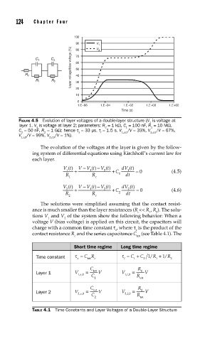
124    Cha pte r  F o u r

                                100
                                90      V
                                         1 2
                              Layer voltage/bias voltage (%)  50
                                        V
                                80
                       C        70
                 C 1
                        2       60
             R c                40
                 R 1   R 2      30
                                20
                                10
                                 0
                                 1.E–06   1.E–04   1.E–02  1.E+00   1.E+02
                                                  Time (s)

          FIGURE 4.5  Evolution of layer voltages of a double-layer structure (V  is voltage at
                                                             1
          layer 1, V  is voltage at layer 2; parameters: R = 1 kΩ, C = 100 nF, R = 10 MΩ,
                 2                          C       1        1
          C = 50 nF, R = 1 GΩ; hence τ = 33 μs, τ = 1.5 s, V  /V = 33%, V  /V = 67%,
           2        2            s        l       1,s,0      2,s,0
          V  /V = 99%, V  /V = 1%).
           1,l,0      2,l,0
                   The evolution of the voltages at the layer is given by the follow-
               ing system of differential equations using Kirchhoff’s current law for
               each layer.
                           Vt ()  VV t ()−  −  V t ()  dV t ()
                             1  +     1    2  +  C  1  =  0          (4.5)
                            R         R          1  dt
                              1         c
                           Vt ()  VV t ()−  −  V t ()  dV t ()
                             2  +     1    2  +  C  2   =  0         (4.6)
                            R         R          2  dt
                             2          c
                   The solutions were simplified assuming that the contact resist-
               ance is much smaller than the layer resistances (R << R , R ). The solu-
                                                        c    1  2
               tions V  and V  of the system show the following behavior: When a
                     1      2
               voltage V (bias voltage) is applied on this circuit, the capacitors will
               charge with a common time constant τ , where τ  is the product of the
                                                s      s
               contact resistance R  and the series capacitance C  (see Table 4.1). The
                                c                       tot
                                Short time regime  Long time regime
                 Time constant  τ =  CR c         τ =  C +  C 1/ R + 1/ R 2
                                                   l
                                                       1
                                     tot
                                 s
                                                               1
                                                          2
                                      C                 R
                 Layer 1        V 1,, s 0  =  tot  V  V 10  =  1  V
                                                    l ,,
                                      C
                                       1                R tot
                                      C                 R
                 Layer 2        V 2,, s 0  =  tot  V  V 2,, l 0  =  2  V
                                      C
                                       2                R tot
               TABLE 4.1  Time Constants and Layer Voltages of a Double-Layer Structure
   142   143   144   145   146   147   148   149   150   151   152