
Page 146 - Organic Electronics in Sensors and Biotechnology
P. 146
Integrated Pyr oelectric Sensors 123
140
120
100
Device thickness (nm) 80
60
40
20
0
–6 –5 –4 –3 –2 –1 0 1 2 3 4 5
Bias voltage (V)
Bulk layer BCB (Young layer)
Depletion layer (Young) BCB (ideal dielectric)
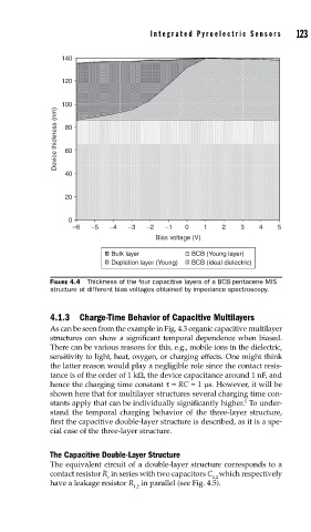
FIGURE 4.4 Thickness of the four capacitive layers of a BCB-pentacene MIS
structure at different bias voltages obtained by impedance spectroscopy.
4.1.3 Charge-Time Behavior of Capacitive Multilayers
As can be seen from the example in Fig. 4.3 organic capacitive multilayer
structures can show a significant temporal dependence when biased.
There can be various reasons for this, e.g., mobile ions in the dielectric,
sensitivity to light, heat, oxygen, or charging effects. One might think
the latter reason would play a negligible role since the contact resis-
tance is of the order of 1 kΩ, the device capacitance around 1 nF, and
hence the charging time constant τ = RC = 1 μs. However, it will be
shown here that for multilayer structures several charging time con-
stants apply that can be individually significantly higher. To under-
5
stand the temporal charging behavior of the three-layer structure,
first the capacitive double-layer structure is described, as it is a spe-
cial case of the three-layer structure.
The Capacitive Double-Layer Structure
The equivalent circuit of a double-layer structure corresponds to a
contact resistor R in series with two capacitors C which respectively
c 1,2
have a leakage resistor R in parallel (see Fig. 4.5).
1,2