
Page 144 - Organic Electronics in Sensors and Biotechnology
P. 144
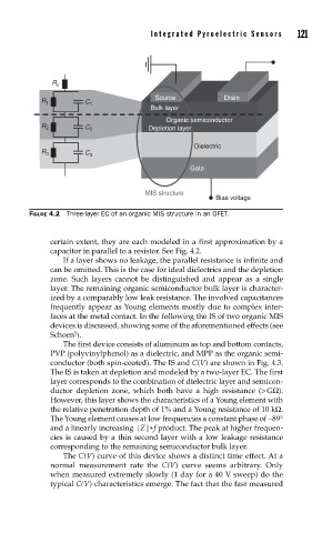
Integrated Pyr oelectric Sensors     121


                R c
                                         Source           Drain
             R 1        C 1
                                        Bulk layer
                                            Organic semiconductor
             R 2        C 2             Depletion layer

                                                   Dielectric
             R 3        C 3
                                                  Gate


                                       MIS structure
                                                        Bias voltage
          FIGURE 4.2  Three-layer EC of an organic MIS structure in an OFET.


               certain extent, they are each modeled in a first approximation by a
               capacitor in parallel to a resistor. See Fig. 4.2.
                   If a layer shows no leakage, the parallel resistance is infinite and
               can be omitted. This is the case for ideal dielectrics and the depletion
               zone. Such layers cannot be distinguished and appear as a single
               layer. The remaining organic semiconductor bulk layer is character-
               ized by a comparably low leak resistance. The involved capacitances
               frequently appear as Young elements mostly due to complex inter-
               faces at the metal contact. In the following the IS of two organic MIS
               devices is discussed, showing some of the aforementioned effects (see
               Schoen ).
                     5
                   The first device consists of aluminum as top and bottom contacts,
               PVP (polyvinylphenol) as a dielectric, and MPP as the organic semi-
               conductor (both spin-coated). The IS and C(V) are shown in Fig. 4.3.
               The IS is taken at depletion and modeled by a two-layer EC. The first
               layer corresponds to the combination of dielectric layer and semicon-
               ductor depletion zone, which both have a high resistance (> GΩ).
               However, this layer shows the characteristics of a Young element with
               the relative penetration depth of 1% and a Young resistance of 10 kΩ.
               The Young element causes at low frequencies a constant phase of −89°
               and a linearly increasing |Z| *  f product. The peak at higher frequen-
               cies is caused by a thin second layer with a low leakage resistance
               corresponding to the remaining semiconductor bulk layer.
                   The C(V) curve of this device shows a distinct time effect. At a
               normal measurement rate the  C(V) curve seems arbitrary. Only
               when measured extremely slowly (1 day for a 40 V sweep) do the
               typical C(V) characteristics emerge. The fact that the fast measured