
Page 145 - Organic Electronics in Sensors and Biotechnology
P. 145
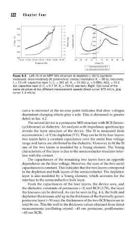
122    Cha pte r  F o u r

                                                       480
                                      –80
             450                      –81              470
                                      –82              460
             430                      –83              450
            Z ·f (kΩ · Hz)  410       –84  Phase (deg)  Capacitance (pF)  440
                                      –85
             390                      –86              430
                                      –87
                                                       420
             370                      –88
                                                       410
                                      –89
             350                      –90              400
             1.E+01 1.E+02 1.E+03 1.E+04 1.E+05 1.E+06 1.E+07  –40  –30  –20  –10  0  10  20  30  40  50
                       Frequency (Hz)                   Voltage (V)
                                                     Measurement time 28 h
                                                     Measurement time 160 s
          FIGURE 4.3  Left: IS of an MPP MIS structure at depletion (−40 V) (symbols–
          measured, lines–modeled) (fi t parameters: contact resistance R = 99 Ω, inductivity
                                                          c
          L = 10 nH; capacitive layer 1: C = 391 pF, R = 10 GΩ; p = 0.98%, R(0) = 10.1
                                  1         1        1          1
          kΩ; capacitive layer 2: C = 5.7 nF, R = 704 Ω, see text). Right: C(V) curve of the
                            2        2
          same structure at two different measurement speeds (black curve: 875 mV/s, gray
          curve: 1.4 mV/s)

               curve is mirrored at the reverse point indicates that slow voltages
               dependent charging effects play a role. This is discussed in greater
               detail in Sec. 4.2.
                   The second device is a pentacene MIS structure with BCB (benzo-
               cyclobutene) as dielectric. An analysis with impedance spectroscopy
               reveals the layer structure of the device. The IS is measured from
               accumulation ( −6 V) to depletion (5 V). They can be fit by four layers:
               two layers have a constant capacitance over the entire bias voltage
               range and hence are attributed to the dielectric. However, to fit the IS
               one of the two layers is modeled by a Young element. The Young
               characteristic of this layer is due to the semiconductor-insulator inter-
               face with the contact.
                   The capacitances of the remaining two layers have an opposite
               dependence on the bias voltage. However, the sum of the two serial
               capacitances is constant. This indicates that the two layers correspond
               to the depletion and bulk layers of the semiconductor. The depletion
               layer is also modeled by a Young element, which accounts for the
               interface to the semiconductive bulk layer.
                   From the capacitances of the four layers, the device area, and
               the dielectric constants of pentacene (~3) and BCB (3.78), the layer
               thicknesses can be derived. As can be seen in Fig. 4.4, the bulk and
               depletion thicknesses add up to the thickness of the thermally grown
               pentacene layer (~50 nm); the thicknesses of the two BCB layers are in
               total 86 nm. This fits well to the thickness values obtained from direct
               measurements (oscillating crystal: ~45 nm pentacene, profilometer:
               ~85 nm BCB).