
Page 159 - Organic Electronics in Sensors and Biotechnology
P. 159
136 Cha pte r F o u r
Diode driver
70
Function generator 60
Laser diode
50
Lock-in I max (nA) 40
Amplifier 30
20
Electrode Ag
10
P(VDF-TrFE) layer
1 2 3 4 5 6 7 8
Poling procedure number
Substrate
400
(a)
350
300
80 mW excitation at 808 nm
U max (mV)
1E–7 250
1 0.1 200
150
Pyroelectric. Aw. (A) 1E–9 0.01 Pyroelectric. Aw. (V) 100 0 1 2 3 4 5 6 7 8
1E–8
50
1E–3
1E–4
1: 250 V (sine) Poling procedure number
5: 500 V (sqr + absorber)
1E–10 1E–10
2: 400 V (sine) 6: 400 V (80°C)
10 –2 10 –1 10 0 10 1 10 2 10 3 10 4 10 5 10 6 3: 500 V (sine) 7: 400 V (100°C)
4: 500 V (sine + absorber) 8: 400 V (130°C)
Frequency (Hz)
(c) (b)
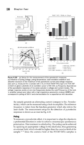
FIGURE 4.10 (a) Setup for the measurement of the pyroelectric response.
(b) Infl uence of poling voltage, poling temperature, laser excitation waveform and
absorber structure on the maximum of the pyroelectric current and voltage response
(see part c), measured for a sample with 2.9 μm thick P(VDF:TrFE) layer and 70% VDF
content on glass substrate at an excitation power of 80 mW. (c) Frequency dependence
of the pyroelectric response of the same sample in voltage and current modes. The
voltage response points at very low frequencies (below the cutoff frequency of the lock-
in amplifi er setup) were taken with a high-impedance parametric analyzer (MBPA) and
correspond to poling at 500 V and sine excitation for a capacitance with absorber.
the sample generate an alternating current (compare to Sec. Pyroelec-
tricity), which can be measured using a lock-in amplifier. The reference
frequency is taken from the function generator which also drives the
laser diode. The measurement setup for the detection of pyroelectric
responses is shown as an inset in Fig. 4.10.
Poling
To measure a pyroelectric effect, it is important to align the dipoles in
a preferential direction in order to achieve a macroscopic spontaneous
polarization. This treatment is called poling. The poling can be achieved
by applying an appropriate voltage to the electrodes, thus generating
an external field, which should be higher than the coercive field of the
sample. 29, 30 Since the coercive field of the P(VDF-TrFE) samples is