
Page 190 - Organic Electronics in Sensors and Biotechnology
P. 190
Progress and Challenges in OLED-Based Chemical and Biological Sensors 167
from a few square microns to several square millimeters, and pixels as
29
small as 60 nm in diameter have been reported. These developments
and their rapid commercialization present an opportunity to develop a
new platform of integrated (micro)sensor arrays.
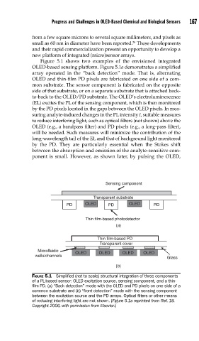
Figure 5.1 shows two examples of the envisioned integrated
OLED-based sensing platform. Figure 5.1a demonstrates a simplified
array operated in the “back detection” mode. That is, alternating
OLED and thin-film PD pixels are fabricated on one side of a com-
mon substrate. The sensor component is fabricated on the opposite
side of that substrate, or on a separate substrate that is attached back-
to-back to the OLED/PD substrate. The OLED’s electroluminescence
(EL) excites the PL of the sensing component, which is then monitored
by the PD pixels located in the gaps between the OLED pixels. In mea-
suring analyte-induced changes in the PL intensity I, suitable measures
to reduce interfering light, such as optical filters (not shown) above the
OLED (e.g., a bandpass filter) and PD pixels (e.g., a long-pass filter),
will be needed. Such measures will minimize the contribution of the
long-wavelength tail of the EL and that of background light monitored
by the PD. They are particularly essential when the Stokes shift
between the absorption and emission of the analyte-sensitive com-
ponent is small. However, as shown later, by pulsing the OLED,
Sensing component
Transparent substrate
PD OLED PD OLED PD
Thin film-based photodetector
(a)
Thin film-based PD
Transparent cover
Microfluidic OLED OLED OLED OLED
wells/channels
Glass
(b)
FIGURE 5.1 Simplifi ed (not to scale) structural integration of three components
of a PL-based sensor: OLED excitation source, sensing component, and a thin-
fi lm PD. (a) “Back detection” mode with the OLED and PD pixels on one side of a
common substrate and (b) “front detection” mode with the sensing component
between the excitation source and the PD arrays. Optical fi lters or other means
of reducing interfering light are not shown. (Figure 5.1a reprinted from Ref. 18.
Copyright 2006, with permission from Elsevier.)