
Page 185 - Organic Electronics in Sensors and Biotechnology
P. 185
162 Cha pte r F o u r
consideration of the measurement circuitry and the input impedance
of the OTFT itself, in that case the total gate voltage V varies from
G;tot
1.5 to −1.5 V, resulting in a variation of the drain current between I =
off
-8
2 × 10 −10 A to the on state at I = 3 × 10 A. Due to the maximum
on
negative V ~ −1.5 V compared to V ~ −2 V that is achieved, if an
G;tot G;tot
additional gate bias of −0.5 V is applied, the on current is somewhat
smaller in this case. This is mainly due to the very steep transition
from off-to-on state intrinsic to the Al O -based OTFTs, meaning that
2 3
a small increase in the V can induce a significant increase in the
mod;eff
on current level.
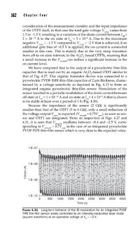
We have compared that to the output of a pyroelectric thin-film
capacitor that is read out by an organic Al O -based OTFT similar to
2 3
that of Fig. 4.27. This organic transistor device was connected to a
pyroelectric PVDF-TrFE thin-film capacitor of 2 μm thickness, charac-
terized by a voltage sensitivity as depicted in Fig. 4.13 to form an
integrated organic pyroelectric thin-film sensor. Stimulation of the
sensor resulted in a periodic modulation of the drain current between
−8
off state at I = 1 × 10 −10 A and on state at I = 4 × 10 A that is shown
off on
to be stable at least over a period of 1 h (Fig. 4.30).
Because the impedance of the sensor (2 GΩ) is significantly
smaller than that of the OTFT (5 to 6 GΩ), only a small reduction of
the voltage output V is expected (V = 0.75V ), as soon as sen-
sens sens;eff sens
sor and OTFT are integrated. From an inspection of Figs. 4.27 and
4.31, it is seen that V oscillates between -0.4 and -2.5 V, corre-
sens;eff
sponding to V ~ 0.7V in the case of an integrated pyroelectric
sens;eff sens
PVDF-TrFE thin-film sensor which is very close to the expected value.
1.E–07
1.E–08
I Drain (A)
1.E–09
1.E–10
0 500 1000 1500 2000 2500 3000 3500 4000
Time (s)
FIGURE 4.31 Long-term behavior of the ID modulation for an integrated PVDF-
TrFE thin-fi lm sensor solely controlled by an intensity-modulated laser diode
(square waveform) at an operation voltage of V =−3 V.
D