
Page 181 - Organic Electronics in Sensors and Biotechnology
P. 181
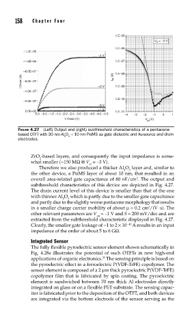
158    Cha pte r  F o u r

                                                 1.E–05
                                                                 V D  = –3 V
                                                 1.E–06
            –1.2E–06
                                          –4 V
            –1.0E–06                             1.E–07
            –8.0E–07                             1.E–08
            I Drain (A)  –6.0E–07         –3 V   I ds (A)  1.E–09

            –4.0E–07
                                                 1.E–10
            –2.0E–07
                                          –2 V
                                          –1 V
             0.0E+00                             1.E–11
                 0.0 –0.5 –1.0 –1.5 –2.0 –2.5 –3.0 –3.5 –4.0 –4.5 –5.0  –4  –3  –2  –1  0  1
                             V Drain (V)                     V (V)
                                                              gs
          FIGURE 4.27  (Left) Output and (right) subthreshold characteristics of a pentacene-
          based OTFT with 30 nm Al O  + 10 nm PαMS as gate dielectric and Au-source and drain
                              3
                             2
          electrodes.
               ZrO -based layers, and consequently the input impedance is some-
                   2
               what smaller (~150 MΩ @ V  = −3 V).
                                       D
                   Therefore we also produced a thicker Al O  layer and, similar to
                                                     2  3
               the other device, a PαMS layer of about 10 nm, that resulted in an
                                                          2
               overall area-related gate capacitance of 80 nF/cm . The output and
               subthreshold characteristics of this device are depicted in Fig. 4.27.
               The drain current level of this device is smaller than that of the one
               with thinner Al O  which is partly due to the smaller gate capacitance
                            2  3
               and partly due to the slightly worse pentacene morphology that results
               in a smaller charge carrier mobility of about μ = 0.2 cm /(V ⋅ s). The
                                                               2
               other relevant parameters are V  = −1 V and S = 200 mV/dec and are
                                          on
               extracted from the subthreshold characteristic displayed in Fig. 4.27.
               Clearly, the smaller gate leakage of ~1 to 2 × 10  −10  A results in an input
               impedance of the order of about 5 to 6 GΩ.
               Integrated Sensor
               The fully flexible pyroelectric sensor element shown schematically in
               Fig. 4.28a illustrates the potential of such OTFTs in new high-end
                                            35
               applications of organic electronics.  The sensing principle is based on
               the pyroelectric effect in a ferroelectric P(VDF-TrFE) copolymer. The
               sensor element is composed of a 2 μm thick pyroelectric P(VDF-TrFE)
               copolymer film that is fabricated by spin coating. The pyroelectric
               element is sandwiched between 70 nm thick Al electrodes directly
               integrated on glass or on a flexible PET substrate. The sensing capac-
               itor is fabricated prior to the deposition of the OTFT, and both devices
               are integrated via the bottom electrode of the sensor serving as the