
Page 179 - Organic Electronics in Sensors and Biotechnology
P. 179
156 Cha pte r F o u r
increase with decreasing surface roughness. For rms-roughness values
below 0.5 nm the pentacene morphology is characterized by dentritic
crystallites of several microns height composed of well-separated
monolayer-high terraces (see Fig. 4.24c).
It turned out that the nanocomposite-pentacene interface is a
much higher-quality interface than the SiO -pentacene one showing
2
up as (1) very low trap densities in the subthreshold region close to
the theoretical limit (small swing or sharp turn-on), (2) low threshold
voltages, (3) high charge carrier mobilities resulting in reasonably
high drain currents at low voltages, and (4) low leakage currents
resulting in high input impedance. In addition it can be shown (see
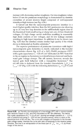
Fig. 4.25) that the interface retains similar high quality if the whole
device is fabricated on flexible substrates. 35
The superior performance of pentacene transistors with high-k
nanocomposite gate dielectrics is clearly indicated in the transfer
characteristics shown Fig. 4.25 of a ZrO /PαMS pentacene OTFT
2
2
with a gate capacitance C = 120 nF/cm fabricated on PET. Note that
i
in the on regime no hysteresis is evident between forward and back-
ward gate voltage sweeps. The off current, however, reveals the
typical gate field behavior with a trianglelike hysteresis. The
37
on/off ratio is deduced from the transfer characteristic I (V ) as
ds gs
6
I = 10 (Fig. 4.25) with the following definitions: I = I (0 V) and
on/off off ds
1.E–05 0.0012
Vd (V): _1 forward
Vd (V): _1 reverse
1.E–06
0.001
1.E–07
0.0008
I Drain (A) 1.E–08 0.0006
1.E–09
0.0004
1.E–10
0.0002
1.E–11
1.E–12 0
–3.5 –2.5 –1.5 –0.5 0.5 1.5
V Gate (V)
(a) (b)
FIGURE 4.25 (a) Transfer characteristics of a low-voltage OTFT with a nanocomposite
gate dielectric based on ZrO and PVCi fabricated on PET fi lm (Melinex). The device
2
2
has a gate capacitance of C = 0.12 μF/cm , proving low-voltage operation (V =−1.3 V)
i T
with a subthreshold swing S ~ 100 mV/dec (forward sweep), which is close to the
theoretical limit of 82 mV/dec. The curve with triangles corresponds to the forward
gate voltage sweep, whereas the curve with dots corresponds to the reverse sweep
direction. The line is an extrapolation of the linear part of I to I = 0. (b) Photo
ds ds
image of this device.