
Page 177 - Organic Electronics in Sensors and Biotechnology
P. 177
154 Cha pte r F o u r
the output signals typically are in the region 0.1 < V < 1 V. So if a
pyro
clear impact of the sensor signal on the OTFT current is desired, the
threshold voltage of the transistor should not be an order of magni-
tude larger. Second, the OTFT input really needs to have a high-
impedance input (~ gigaohms) in order not to unwillingly downscale
the sensor signal. That means basically that the gate dielectric has to
be very dense with low leakage currents and sufficiently high break-
down strengths. Third, the overall performance and stability should
be sufficient for the targeted application (that could be an interesting
point in the case of automotive industry driven applications). And
last but not least, the fabrication process should be compatible with
large-area processing on flexible substrates, thus arguing for printing
and large-area evaporation techniques.
Low-Voltage OTFTs
Reducing the threshold voltage and also the subthreshold swing is
essential for operating OTFTs at low-voltage levels. When combined
with very low gate leakage currents, OTFTs may also become a key
element in high-end sensor applications, such as flexible touchpads
and screens or thermal imaging tools for night vision, surveillance, or
for the detection of undesired heat loss paths in buildings.
The aforementioned transistor parameters critically depend on
not only the thickness and the dielectric properties of the gate insula-
tor, but also the trapped charge densities at the interface between
these materials. The selection of semiconductors and gate insulators
33
with excellent interface properties is currently the challenge in the
quest for improving the performance of OTFTs.
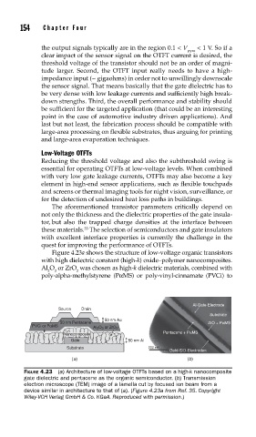
Figure 4.23a shows the structure of low-voltage organic transistors
with high dielectric constant (high-k) oxide–polymer nanocomposites.
Al O or ZrO was chosen as high-k dielectric materials, combined with
2 3 2
poly-alpha-methylstyrene (PαMS) or poly-vinyl-cinnamate (PVCi) to
Al-Gate-Electrode
Source Drain
Substrate
50 nm Au
50 nm Pentacene ZrO + PαMS
PVCi or PαMS
Al 2 O 3 or ZrO 2
Nanocomposite Pentacene + PαMS
Gate 50 nm Al
Substrate 200 nm
Gold-S/D-Electroden
(a) (b)
FIGURE 4.23 (a) Architecture of low-voltage OTFTs based on a high-k nanocomposite
gate dielectric and pentacene as the organic semiconductor. (b) Transmission
electron microscope (TEM) image of a lamella cut by focused ion beam from a
device similar in architecture to that of (a). (Figure 4.23a from Ref. 35. Copyright
Wiley-VCH Verlag GmbH & Co. KGaA. Reproduced with permission.)